Glass-glass composite optical wave guide

A composite light and glass technology, applied in the field of optical waveguide, can solve the problem that the function of the functional glass substrate 2 cannot be fully exerted, and achieve the effects of multi-functionality, large design and production, and miniaturization

Inactive Publication Date: 2007-08-22
ZHEJIANG UNIV
View PDF0 Cites 6 Cited by
  • Summary
  • Abstract
  • Description
  • Claims
  • Application Information

AI Technical Summary

Problems solved by technology

Generally speaking, in order to ensure the formation of the optical waveguide, the refractive index of the functional glass substrate 2 in this structure must be lower than the refractive index of the light guiding region 3 in the glass substrate 1, which makes the light energy transmitted in the optical waveguide larger. Some of them are distributed near the light guide area 3 in the glass substrate 1, while the energy distributed in the functional glass substrate 2 is very little, as shown in the isointensity line 4 of the optical waveguide mode field distribution in Fig. 1, this distribution feature makes The function of the functional glass substrate 2 (such as light amplification) cannot be fully exerted

Method used


Image

  • Glass-glass composite optical wave guide
  • Glass-glass composite optical wave guide

Examples


Embodiment 1

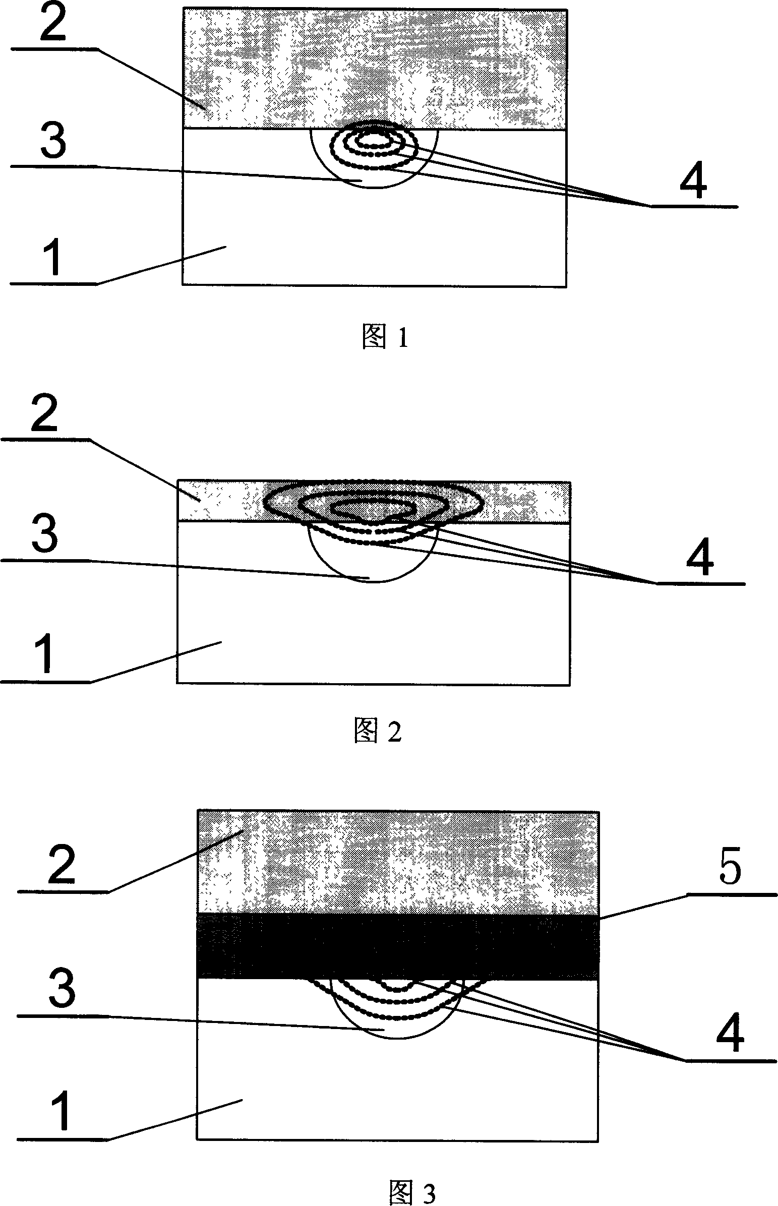
[0024] Embodiment 1: Composite optical waveguide structure see Figure 3, the main process steps

[0025] The glass substrate 1 is made of silicate optical glass material, and the functional glass substrate 2 is made of phosphate glass doped with rare earth. The main manufacturing steps of the glass-glass composite optical waveguide structure:

[0026] (A) Preparation of light guide region 3 on glass substrate 1

[0027] ·Using microfabrication technology to fabricate strip-shaped optical waveguide masks on glass substrates to obtain ion-exchange windows with a width of the order of microns;

[0028] ·Molten salt ion exchange process is used to make strip optical waveguide, and the ion exchange temperature is 300-400°C;

[0029] • Annealing of optical waveguides.

[0030] (B) Preparation of light confinement region 3 on functional glass substrate 2

[0031] · Fabricate the light confinement region 5 on the functional glass substrate 2 by using molten salt ion exchange techn...

Embodiment 2

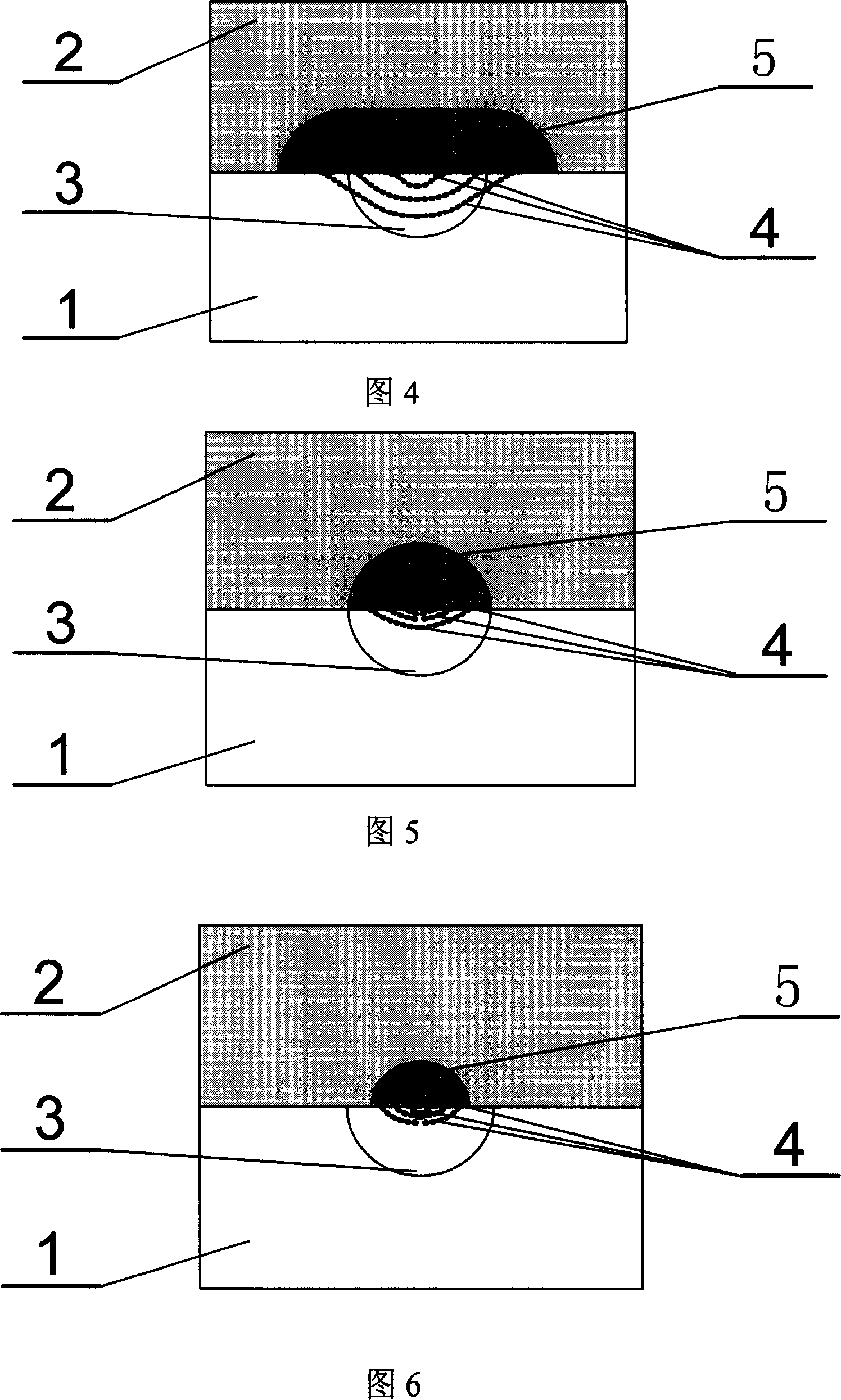
[0034] Embodiment 2: The composite optical waveguide structure is shown in Figure 4, the main process steps

[0035] The glass substrate 1 is made of silicate optical glass material, and the functional glass substrate 2 is made of phosphate glass doped with rare earth. The main manufacturing steps of the glass-glass composite optical waveguide structure:

[0036] (A) Preparation of light guide region 3 on glass substrate 1

[0037] ·Using microfabrication technology to fabricate strip-shaped optical waveguide masks on glass substrates to obtain ion-exchange windows with a width of the order of microns;

[0038] ·Molten salt ion exchange process is used to make strip optical waveguide, and the ion exchange temperature is 300-400°C;

[0039] • Annealing of optical waveguides.

[0040] (B) Preparation of light confinement region 3 on functional glass substrate 2

[0041] ·Using microfabrication technology to fabricate the mask of the strip optical waveguide on the glass subst...

Embodiment 3

[0045] Embodiment 3: Composite optical waveguide structure see Figure 5 and Figure 6, the main process steps

[0046] The glass substrate 1 is made of silicate optical glass material, and the functional glass substrate 2 is made of phosphate glass doped with rare earth. The main manufacturing steps of the glass-glass composite optical waveguide structure:

[0047] (A) Preparation of light guide region 3 on glass substrate 1

[0048] ·Using microfabrication technology to fabricate strip-shaped optical waveguide masks on glass substrates to obtain ion-exchange windows with a width of the order of microns;

[0049] ·Molten salt ion exchange process is used to make strip optical waveguide, and the ion exchange temperature is 300-400°C;

[0050] • Annealing of optical waveguides.

[0051](B) Preparation of light confinement region 3 on functional glass substrate 2

[0052] ·Using microfabrication technology to fabricate strip-shaped optical waveguide masks on glass substrates t...


PUM


Abstract

The invention discloses a glass-glass combined light waveguide, comprising glass substrate with light guiding region and functional glass substrate interlinked, where the functional glass substrate has light limit region and the light guide region and the light limit region together compose core part of the combined light waveguide; even if on the condition that the refractivity of the functional glass substrate is higher than that of the light guide region, by the action of the light limit region, the light transmitted in the light waveguide can not be transmitted in the form of radiation mode. In this case, it assures interaction between the transmitted light and the functional glass substrate and has simple making process; the functional glass substrate has light amplification, nonlinear, magneto-optical or electrooptical property, and this light waveguide structure makes full use of the functions of the functional glass substrate. And the combined waveguide can integrate different functions into the same light waveguide component, implementing miniaturized and multifunctional light integration devices.

Description

technical field [0001] The invention relates to an optical waveguide, in particular to a glass-glass composite optical waveguide. Background technique [0002] Integrated optical circuit means that on the surface of the same substrate, optical waveguides are made of materials with a slightly higher refractive index, and various optical devices such as light sources and gratings are made on this basis. Through this integration, the miniaturization, weight reduction, stabilization and high performance of the optical system can be realized. [0003] The commonly used integrated optical device preparation processes can be divided into two categories: one is the deposition method, including plasma enhanced chemical vapor deposition (PECVD), flame hydrolysis (FHD), sol-gel method (sol-gel), etc. Among them, the PECVD method is the most commonly used; the other is the diffusion method, including metal diffusion on the lithium niobate substrate, proton exchange, and ion exchange on...

Claims


Application Information

Patent Timeline
Patent Type & Authority Applications(China)
IPC IPC(8): G02B6/12G02B1/00
Inventor 郝寅雷江晓清杨建义周强李锡华王明华
Owner ZHEJIANG UNIV
Why Eureka
Try Eureka