Microstructure, semiconductor device, and manufacturing method of the microstructure

一种制造方法、微结构的技术,应用在半导体/固态器件制造、半导体器件、微结构技术等方向,达到防止不良、提高成品率和可靠性、提高耐久性的效果

Inactive Publication Date: 2007-09-12
SEMICON ENERGY LAB CO LTD
View PDF3 Cites 24 Cited by
  • Summary
  • Abstract
  • Description
  • Claims
  • Application Information

AI Technical Summary

Problems solved by technology

[0017] However, in Patent Document 1, the etching method is limited to vapor phase etching
In addition, in Patent Document 2, since the anodization method is used to provide unevenness on the silicon surface when etching the sacrificial layer or after etching the sacrificial layer, it is limited to materials to which the anodization method can be applied.

Method used


Image

  • Microstructure, semiconductor device, and manufacturing method of the microstructure
  • Microstructure, semiconductor device, and manufacturing method of the microstructure
  • Microstructure, semiconductor device, and manufacturing method of the microstructure

Examples


Embodiment approach 1

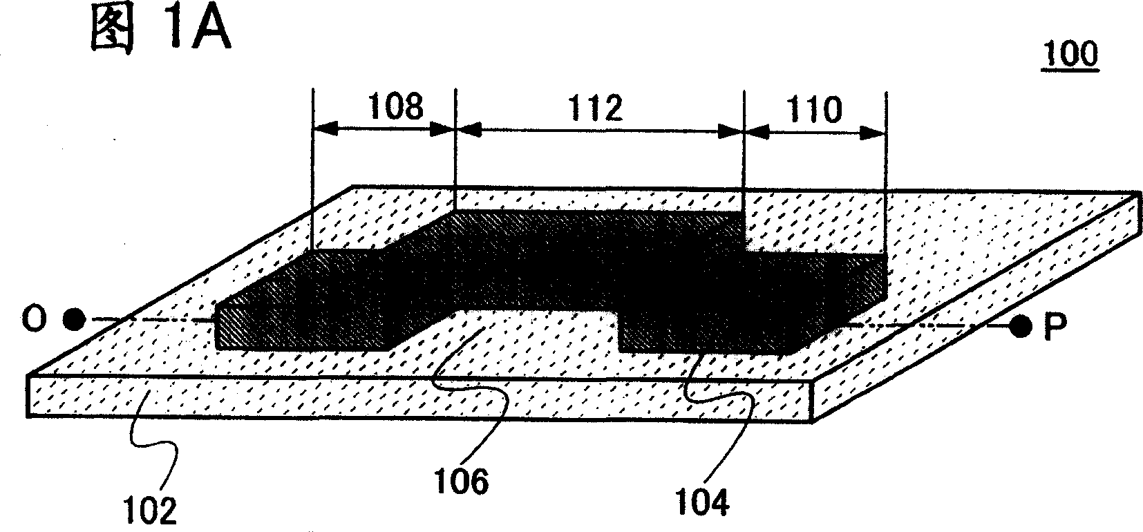
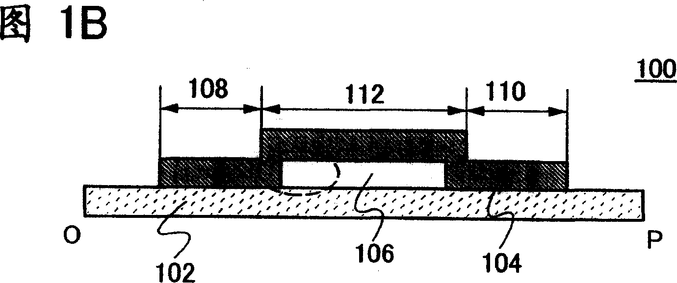
[0050] In this embodiment mode, an example of the microstructure of the present invention will be described with reference to FIGS. 1A to 1C . The microstructure shown in this embodiment is a so-called beam-column structure.

[0051] A perspective view and a cross-sectional view of the microstructure of the present invention are shown in FIG. 1A and FIG. 1B , respectively. FIG. 1B corresponds to a cross-sectional view along the dotted line O-P in FIG. 1A.

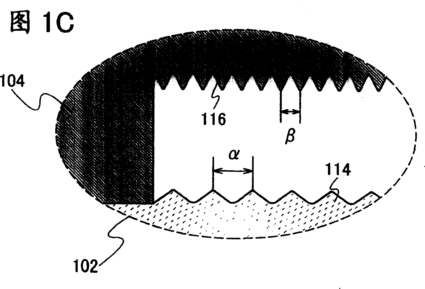
[0052] The microstructure 100 of the present invention includes a first structural layer 102 and a second structural layer 104 . Furthermore, there is a gap 106 between the first structural layer 102 and the second structural layer 104 .

[0053] The second structural layer 104 includes supporting parts 108 , 110 , and a movable part 112 , and is a three-dimensional bridge structure relative to the first structural layer 102 . Specifically, the second structural layer 104 includes support portions 108 , 110 that are in c...

Embodiment approach 2

[0065] An example of the manufacturing method of the microstructure of the present invention will be described with reference to FIGS. 2A to 2D and FIGS. 3A to 3D .

[0066] First, a substrate 200 having an insulating surface is prepared. Next, a base insulating film 202 is formed over the substrate 200 (FIG. 2A). Examples of the substrate 200 having an insulating surface include a glass substrate, a quartz substrate, a plastic substrate, and the like. Lightweight, flexible and thin devices can be obtained by forming microstructures on plastic substrates. In addition, thin devices can also be obtained by thinning the glass substrate by grinding or the like. In addition, a substrate in which an insulating film is formed on a conductive substrate such as metal or a semiconductor substrate such as silicon can also be used.

[0067] As the base insulating film 202, a material such as silicon oxide, silicon nitride, silicon nitride containing oxygen, or silicon oxide containing ...

Embodiment approach 3

[0092] In this embodiment mode, a case where aluminum is used for the sacrificial layer will be described with reference to FIGS. 4A to 4E . Note that materials, manufacturing methods, and the like other than the sacrificial layer are the same as those in Embodiment Mode 2 above. Note that in this embodiment, only a single-ended cantilever beam structure (cantilever) in which only a structural layer having a movable portion (structural layer formed on a sacrificial layer) is fixed is employed.

[0093] First, similarly to the second embodiment, the first structure layer 206 is formed. Next, an aluminum film 309 is formed on the first structure layer 206 by using a sputtering method (FIG. 4A). Note that a stacked structure of other metals and aluminum films may also be used. Note that in the case of a stacked structure, the aluminum film should be the upper layer.

[0094] Next, surface roughening is performed on the surface of the aluminum film 309 . Through this surface r...


PUM


Abstract

A microstructure includes a first structural layer and a second structural layer which faces the first structural layer with a space interposed therebetween and is partially fixed to the first structural layer. At least one of the first structural layer and the second structural layer can be displaced. Further, opposed surfaces of the first structural layer and the second structural layer are different in roughness.

Description

technical field [0001] The present invention relates to microstructures and methods for their manufacture. Background technique [0002] Previously, research into the manufacture of micromachines has been conducted using semiconductor element manufacturing processes and methods similar to this. For example, by processing a silicon wafer, a three-dimensional structure such as a gear or a bridge structure having a cavity and a portion movable in the cavity is manufactured. [0003] In recent years, studies have been conducted on the manufacture of tiny electromechanical devices with one function by manufacturing the above-mentioned structure and semiconductor elements on the same substrate, or bonding separately manufactured structures and semiconductor elements together. device. These are called MEMS (Micro Electro Mechanical System), micromachines, micromachining, and the like. [0004] Such minute electromechanical devices (micromachines) are broadly classified into the ...

Claims


Application Information

Patent Timeline
Patent Type & Authority Applications(China)
IPC IPC(8): B81B5/00H01L29/94H01L27/00H01L49/00B81C1/00H01L21/02
CPCB81B3/0013H01L27/1266B81B3/001B81C2201/115H01L27/1214H01L29/00
Inventor 山口真弓泉小波
Owner SEMICON ENERGY LAB CO LTD
Why Eureka
Try Eureka