Organic ultraviolet detector

An organic ultraviolet light and detector technology, which is applied in the direction of photometry using electric radiation detectors, can solve the problems of high cost, inapplicability to large-area applications, and complicated preparation process of inorganic ultraviolet light detectors, achieving small size, light weight effect

Inactive Publication Date: 2007-10-17
CHANGCHUN INST OF OPTICS FINE MECHANICS & PHYSICS CHINESE ACAD OF SCI
View PDF1 Cites 29 Cited by
  • Summary
  • Abstract
  • Description
  • Claims
  • Application Information

AI Technical Summary

Problems solved by technology

Due to the complex preparation process and high cost of inorganic ultraviolet photodetectors, they are not suitable for large-area applications[1-2]

Method used


Image

  • Organic ultraviolet detector

Examples


Embodiment 1

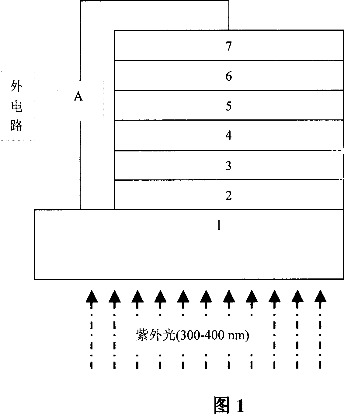
[0030] The utility model selects the device structure shown in Fig. 1 for use. In the present embodiment, at first the transparent conductive film 2 selects the ITO film as the hole collecting electrode, and after cleaning the transparent conductive film 2 on the substrate 1, at first it is cleaned in a high vacuum (3-2×10 -4Pa), on the transparent conductive film 2, deposit a layer of thickness of 10nm electron donor layer 3TPD, and then deposit electron donor TPD and electron acceptor PBD ratio on the electron donor layer 3 with a ratio of 1:1 and a thickness of 5nm. The mixed layer 4 and the electron acceptor layer 5 are deposited on the mixed layer 4 with a thickness of 10nm or 20nm or 30nm. Afterwards, the electron collecting layer 6 is deposited, and the material is LiF, and its thickness is 0.8nm; finally, the electron collecting electrode 7 is deposited, and the metal Al material is used. All of the above films were deposited using thermal evaporation processes. The ...

Embodiment 2

[0033] On the basis of Example 1, the electron donor layer is selected from the m-MTDATA material, and the thickness is 10nm, and then the electron donor m-MTDATA and the electron acceptor Gd (DBM) are deposited on the layer 3 3 The phen ratio is 1:1, the mixed layer 4 with a thickness of 5nm, and then the electron acceptor layer Gd (DBM) is deposited on the mixed layer 4 3 The thickness of phen5 is selected as 10nm or 20nm or 30nm. Afterwards, the electron collecting layer 6 is deposited, and the material is LiF, and its thickness is 0.8nm; finally, the electron collecting electrode 7 is deposited, and the metal Al material is used. All of the above films were deposited using thermal evaporation processes. The thickness of the film is monitored with a film thickness monitoring instrument, and the open circuit voltage and short circuit current are detected with a voltage-ammeter. When irradiating with one side of the ultraviolet photoconductive film 2 and using an external c...

Embodiment 3

[0036] On the basis of Example 1, the hole collection layer 3 is made of m-MTDATA material with a thickness of 10 nm, a mixed layer 4 with a ratio of m-MTDATA and PBD of 1:1 and a thickness of 5 nm, and then electron acceptors are deposited on the mixed layer 4 The thickness of the layer PBD5 is selected to be 10nm or 20nm or 30nm. Other manufacturing conditions remain unchanged. Effect: the power is 4mW / cm 2 When the central wavelength is 365nm UV light irradiation, the electrical signal that can be obtained is; open circuit voltage Voc=2.0V short circuit current Jsc=49μA / cm 2 , When visible light longer than 400nm is irradiated from the side of the ITO transparent electrode, no electrical signal can be detected.


PUM


Abstract

The invention belongs to the material and component field of organic ultraviolet detector comprising a substrate, a transparent conductive film, an electronic donor layer, a mixing layer, an electronic receptor layer, and an electronic collection electrode layer, characterized in that: the thin mixing layer of electronic donor and electronic receptor is disposed between the electronic donor layer and the electronic receptor layer, and the absorption band of the used functional material is located in the ultraviolet region of 300-400nm, the UV light with center wavelength of 365nm are used as UV light source. The organic light detector is organic photovoltaic diode which is sensitive to ultraviolet light and not sensitive to the visual light, can be applicable in the science, industry and business field with simple fabricating process, cheap material and component, small volume, and convenience for carrying, therefore tending to be used widely.

Description

technical field [0001] The invention belongs to the field of ultraviolet-sensitive organic photovoltaic diodes or organic ultraviolet light detection devices, and relates to obtaining a device structure that is only sensitive to ultraviolet (UV-A: 320-400nm) but insensitive to visible light. Background technique [0002] It is known that Chinese utility model patent No. 96247084 discloses "an infrared photodetector", but no patent application related to "organic ultraviolet detector" has been found yet. Due to the complex preparation process and high cost of inorganic ultraviolet photodetectors, they are not suitable for large-area applications [1-2]. The manufacturing cost of the organic ultraviolet light detector is low, the manufacturing substrate can be freely selected, and it can be made portable because of its light weight. It can be deduced from this that its application prospect and huge potential market have become the hot pursuit of various countries. The photon-...

Claims


Application Information

Patent Timeline
Patent Type & Authority Applications(China)
IPC IPC(8): G01J1/42
Inventor 李文连初蓓陈丽莉毕德锋孔治国
Owner CHANGCHUN INST OF OPTICS FINE MECHANICS & PHYSICS CHINESE ACAD OF SCI
Why Eureka
Try Eureka