Semiconductor light-emitting device and method for separating semiconductor light-emitting devices

A light-emitting device and semiconductor technology, which is applied in the direction of semiconductor devices, semiconductor/solid-state device manufacturing, electric solid-state devices, etc., can solve the problems of increasing the manufacturing cost of light-emitting devices, achieve the effect of shortening the processing time and increasing the production volume of devices

Inactive Publication Date: 2007-12-05
TOYODA GOSEI CO LTD
View PDF4 Cites 40 Cited by
  • Summary
  • Abstract
  • Description
  • Claims
  • Application Information

AI Technical Summary

Problems solved by technology

Thereby increasing the manufacturin

Method used


Image

  • Semiconductor light-emitting device and method for separating semiconductor light-emitting devices
  • Semiconductor light-emitting device and method for separating semiconductor light-emitting devices
  • Semiconductor light-emitting device and method for separating semiconductor light-emitting devices

Examples


example 1

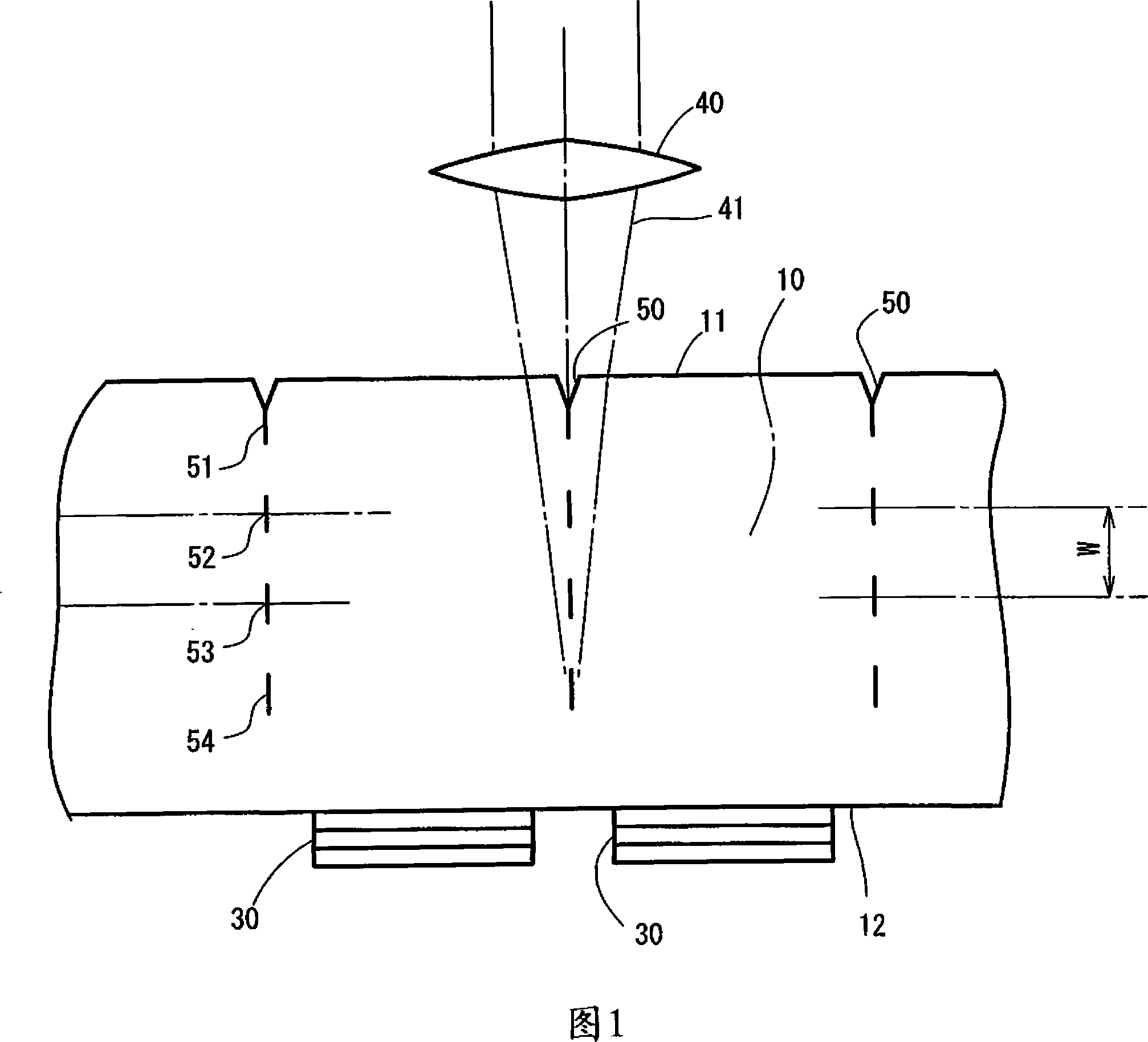
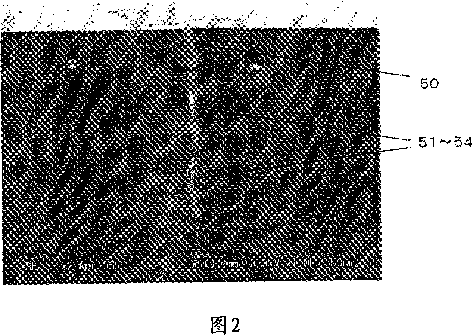
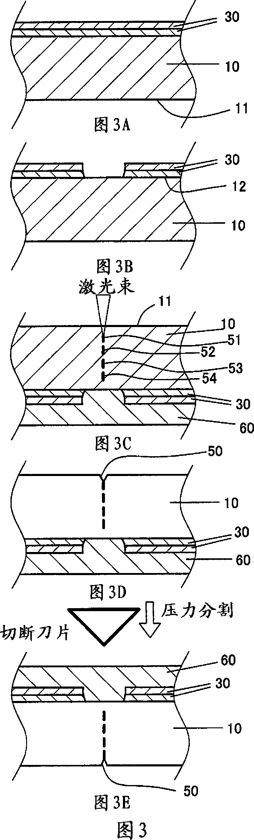
[0091] 3A to 3E illustrate steps included in a method for separating semiconductor light emitting devices according to a specific example of the present invention. As shown in FIG. 3A , a semiconductor light emitting device 30 based on a group III nitride compound was formed on one surface 12 of a sapphire substrate 10 having a thickness of 140 μm through epitaxial growth, electrode formation, and other steps. Subsequently, portions near the division lines unnecessary for separating the group III nitride compound-based semiconductor light emitting device 30 are removed by etching (FIG. 3B).

[0092] Next, an adhesive tape (adhesive tape) 60 is attached to the surface of the sapphire substrate 10 on which the semiconductor light emitting device 30 based on the group III nitride compound is formed, and the femtosecond pulsed laser beam is placed on the surface as the back surface of the sapphire substrate 10 11, thereby forming the groove 50 and the structurally modified portion...

Embodiment 2

[0101] Example 2 relates to a method for separating light-emitting diode chips according to the invention. Figure 7 shows a configuration of an LED in which a light emitting diode chip is mounted on a support and processed according to one embodiment of the present invention. It is worth noting that Figure 7 is a schematic view, and the lateral / vertical dimensions and layer thicknesses do not reflect actual values. Actually, the transparent substrate 101 has a thickness on the order of about 100 μm, and the semiconductor layer 102 which is a stacked layer including a light emitting layer has a thickness of about 1 μm. The LED chip 103 includes a transparent substrate 101 and a semiconductor layer 102 . The adopted transparent substrate 101 is made of sapphire. The semiconductor layer 102 which is a stacked nitride semiconductor layer including a light emitting layer is formed on the first surface 111 ′ of the sapphire substrate 101 , while the second surface 111 of the trans...

example 2

[0156] As shown in Figure 16, internal embrittlement steps 1 to 19 are performed sequentially. Then, steps 20 and 21 are performed to form the grooves. The process is carried out under the following conditions:

[0157] Workpiece: Sapphire single crystal (thickness: t=500μm)

[0158] Laser equipment: mode-locked fiber laser-based femtosecond laser equipment doped with Er and Yb at the same time

[0159] Wavelength: 1.045μm

[0160] Pulse width: 400fs

[0161] Pulse repetition frequency: 100kHz

[0162] Condenser lens: numerical aperture 0.65, and focal length 4mm

[0163] Pulse energy after condenser lens: 1.5μJ

[0164] Energy flow at the waist: 160J / cm 2 (Calculated)

[0165] Power density at the waist: 400TW / cm 2 (Calculated)

[0166] Laser beam incident surface: c-plane of sapphire crystal (second surface 111 in FIG. 16 )

[0167] Laser beam incident direction: orthogonal to the C-plane (the direction indicated by the white arrow in Figure 16)

[0168] Number o...


PUM

PropertyMeasurementUnit
Thicknessaaaaaaaaaa
Diameteraaaaaaaaaa
Lengthaaaaaaaaaa

Abstract

The invention provides a method for separating semiconductor light-emitting devices formed on a substrate. In the method, a pulse laser beam having a pulse width less than 10 ps in a substrate is focused on the substrate, to thereby cause multi-photon absorption in the substrate. Through multi-photon absorption, a groove is formed through the pulse laser beam along a split line predetermined on a surface of the substrate, the groove being substantially continuous in the direction of the predetermined split line. In addition, internal structurally changed portions are formed through the pulse laser beam at a predetermined depth of the substrate on a predetermined split face, the structurally changed portions being discontinuous in the direction of the predetermined split line. Subsequently, an external force is applied to thereby form a split face along the continuous groove and the discontinuous internal structurally changed portions, whereby the semiconductor light-emitting devices are separated from one another.

Description

technical field [0001] The present invention relates to a method for separating semiconductor light emitting devices formed on a substrate to thereby obtain individual semiconductor light emitting devices, the method comprising separating or singulating a wafer formed of the substrate and the devices disposed thereon. The present invention is particularly effective for isolating semiconductor light emitting devices such as Group III nitride based compounds. The term "wafer" used herein refers to a substrate provided by performing so-called wafer processes such as cleaning, diffusion ion-implantation, thin film growth, epitaxial growth, photolithography, and electrode formation on a transparent substrate. Background technique [0002] Hitherto, various methods for dividing a wafer having semiconductor light emitting devices based on group III nitride compounds on a sapphire substrate to thereby obtain individual semiconductor light emitting devices have been proposed. Typica...

Claims


Application Information

Patent Timeline
IPC IPC(8): H01L33/00H01L21/78B23K26/00B28D5/00B23K26/364B23K26/38H01L33/22H01L33/58H01S3/00
CPCB23K26/0057B23K26/53H01L2224/48091H01L2224/48247H01L2224/48257H01L2224/49107H01L2224/73265H01L2924/00014
Inventor 前田将笹木隆一郎
Owner TOYODA GOSEI CO LTD
Why Eureka
Try Eureka