Large area periodic array three-dimensional microstructure preparation method

A periodic array and microstructure technology, applied in microstructure technology, microstructure devices, manufacturing microstructure devices, etc., can solve the problems of low production efficiency, high production cost, and complex production process of large-area three-dimensional microstructures, and achieve production Low cost, convenient production, suitable for mass production

Inactive Publication Date: 2008-01-09
SHANDONG UNIV
View PDF0 Cites 41 Cited by
  • Summary
  • Abstract
  • Description
  • Claims
  • Application Information

AI Technical Summary

Problems solved by technology

[0004] The purpose of the present invention is to solve the current problems of complex manufacturing process, high production cost and low production efficiency of large-area three-dimensional microstructures, and provide a three-dimensional large-area periodic array with the advantages of low production cost, simple process, and suitable for mass production. Microstructure preparation method

Method used


Image

  • Large area periodic array three-dimensional microstructure preparation method
  • Large area periodic array three-dimensional microstructure preparation method
  • Large area periodic array three-dimensional microstructure preparation method

Examples


Embodiment Construction

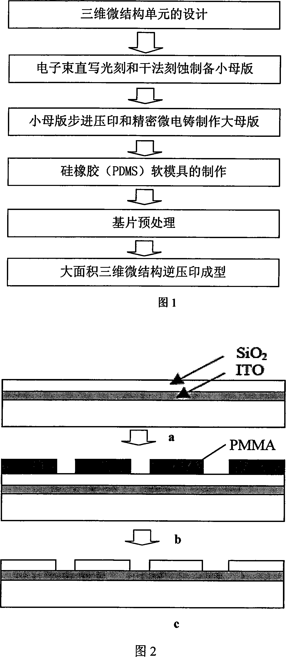
[0051] The present invention will be further described below in conjunction with the accompanying drawings and embodiments.

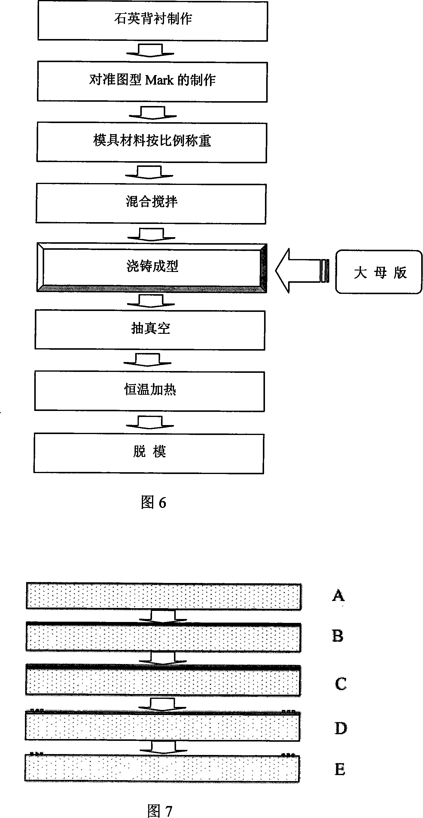
[0052]The molds used in nanoimprinting can be divided into soft molds and hard molds according to the hardness of the material. The surface energy of the hard mold material is high, which is similar to the surface energy of the cured resist, so it is prone to adhesion and difficult to release the mold. In actual use, a release agent must be sprayed on the surface of the mold, which greatly affects the imprinting efficiency. Moreover, sticking is prone to occur even if a release agent is sprayed. It is especially difficult to release large-area three-dimensional microstructures. In addition, due to the parallelism error and flatness tolerance between the substrate surface and the hard mold surface, the contact effect between the hard mold and the substrate surface is poor, and the effective area for pattern conversion is also limited. Compared with th...


PUM


Abstract

The invention discloses a large-area periodical array 3D microstructure preparing method, based on UV nano press printing technique, adopting soft mould and inverse pressure printing to implement low-cost preparation of large-area periodical array 3D microstructure and its basic process flow includes: 1. making small master by electron beam direct write photoetching and dry etching; 2. making large master by small master step-pressure printing and accurate micro-electroforming; 3. pouring liquid PDMS material to large master by vacuum assistance to make silicon rubber soft mould; 4. using quartz glass as substrate and making anti-adhesion surface preprocessing on the substrate; 5. using the ready-made silicon rubber soft mould, and combining with the inversing pressure printing to prepare large area periodical array 3D microstructure on the substrate. And the method has advantages of low cost, process simple, suitable to large batch production, and low cost preparation.

Description

technical field [0001] The invention relates to a method for preparing a microstructure, in particular to a method for preparing a low-cost large-area periodic array three-dimensional microstructure. Background technique [0002] With the in-depth development of micro-electromechanical systems (MEMS) technology, the materials and structures that make up micro-systems are becoming more and more complex. Many MEMS devices such as micro-optical devices, microfluidic devices, micro-fuel cell bipolar plates, and flexible solar cells have increasingly urgent needs for the preparation of large-area three-dimensional microstructures. The large-area three-dimensional microstructures contained in these MEMS devices are usually formed by periodic arrays of many small three-dimensional microstructure units with the same structure. For example, studies on the flow field of bipolar plates at home and abroad have confirmed that compared with existing rectangular, trapezoidal or triangular...

Claims


Application Information

Patent Timeline
Patent Type & Authority Applications(China)
IPC IPC(8): G03F7/00B81C1/00B81C5/00B81C99/00
Inventor 兰红波丁玉成
Owner SHANDONG UNIV
Why Eureka
Try Eureka