Method of manufacturing flip welding LED chip

A technology of light-emitting diodes and a manufacturing method, which is applied to electroluminescent light sources, light sources, electric light sources, etc., can solve the problems of low yield, complicated process, and unreliable combination of LED chips and substrates, and achieves favorable heat dissipation and cost reduction. Effect

Active Publication Date: 2008-02-06
HC SEMITEK SUZHOU
View PDF0 Cites 1 Cited by
  • Summary
  • Abstract
  • Description
  • Claims
  • Application Information

AI Technical Summary

Problems solved by technology

There have been many technologies used to manufacture flip-chip LED chips, but the existing flip-chip LED chips generally have problems such as complex process, low yield, and unreliable combination of LED chips and substrates, and need to use Complicated and expensive flip-chip equipment, for these reasons, the technology of flip-chip LED chips has not been widely used in the manufacturing field

Method used


Image

  • Method of manufacturing flip welding LED chip
  • Method of manufacturing flip welding LED chip

Examples


Embodiment 1

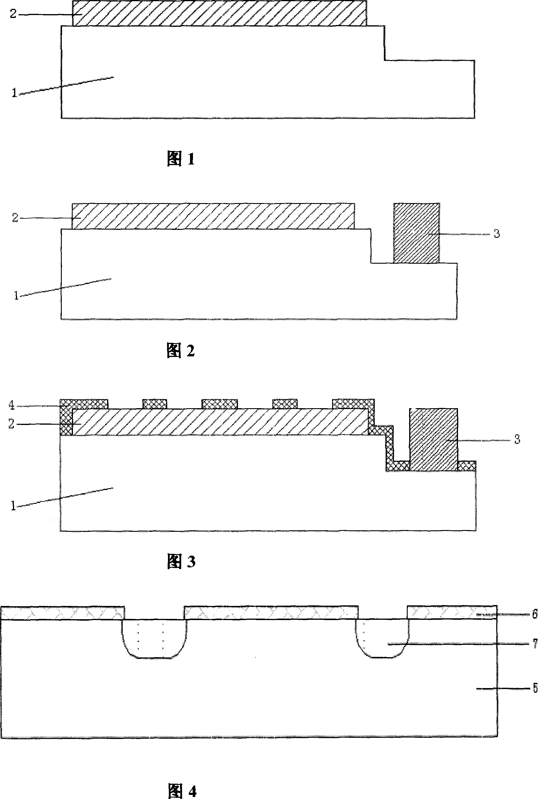
[0024] Step 1, taking the manufacture of GaN LED chips as an example, start the following process steps from the GaN epitaxial wafer:

[0025] 1. Etch GaN first, then vapor-deposit metal Ag to make P electrodes and reflective layers; (Figure 1)

[0026] 2. Evaporate metal Ti and Zn, make N electrode, etch, and separate P electrode and N electrode; (Figure 2)

[0027] 3. Evaporate silicon dioxide to make a passivation layer; (Figure 3)

[0028] Step 2: Substrate process, taking the silicon substrate as an example, perform the following process steps:

[0029] 1. Silicon oxidation, photolithography, SiO 2 Etching, ion implantation or diffusion; (Figure 4)

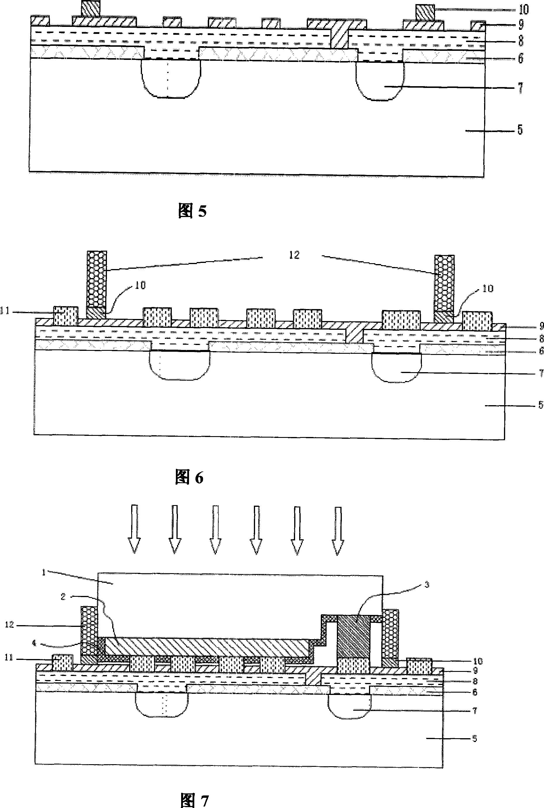
[0030] 2. Evaporation of metal, photolithography, fabrication of electrodes, deposition of SiO 2 , lithography, etch SiO 2 , exposing part of the metal, used to make "bumps" and "walls" of metal electrodes; The effect is similar, but it is continuous in this embodiment, which is to improve the light-gathering and heat-d...


PUM


Abstract

The present invention is a flip chip bonding LED chip preparation method. The present invention is characterized in that the method comprises the steps as follows: (1) make an LED chip B according to the LED chip manufacturing technology, and a metal reflective layer is vapor deposed on the tabling face of the chip B, which not only makes the current more even, but also makes the light be reflected from the back of the LED chip; (2) make a chip A with proper size according to the chip B; a metal convex point and a metal fence are made on the chip A through the manufacturing technology of photolithography, electroplating and evaporation; put the chip B into the fence of the chip A, and the chip B and the chip A are reliably combined with each other through pressuring and heating. The present invention simplifies the manufacturing technology of the flip chip bonding LED chip and increases the reliability of the chip, thereby increasing the yield, without complex device, so that greatly reducing the production cost. The present invention can be used in the mass production of the LED chip, expressly of the high power LED chip.

Description

technical field [0001] The invention provides an improved manufacturing method of flip-chip welding light-emitting diode chips, especially for the manufacture of high-power light-emitting diodes. Background technique [0002] Flip-chip light-emitting diode (LED) chips generally refer to the combination of an LED chip (such as a gallium nitride GaN LED) and a substrate (such as a Si chip). Flip-chip can better solve two problems in LED chips: heat dissipation and antistatic. The reason is that the thermal conductivity of the substrate is good, which can help the heat dissipation of the LED chip. At the same time, antistatic protection diodes are manufactured on the substrate. It can be used to improve the antistatic ability of the LED chip, thereby improving the reliability of the LED chip. [0003] Flip-chip is mainly used in the manufacture of high-power (power greater than or equal to 1 watt) LEDs, because high-power LED chips have higher requirements for heat dissipation...

Claims


Application Information

Patent Timeline
Patent Type & Authority Applications(China)
IPC IPC(8): H05B33/10H01L33/00
Inventor 鲍坚仁应华兵张建宝曾灵琪
Owner HC SEMITEK SUZHOU
Why Eureka
Try Eureka