Substrate processing system, gas supply unit, method of substrate processing, computer program, and storage medium

A technology of a substrate processing device and a substrate processing method, which is applied in the fields of electrical components, electrical program control, semiconductor/solid-state device manufacturing, etc., can solve the problems of increasing the deposition amount and failing to improve the in-plane size distribution of lines, etc., to achieve The effect of improving in-plane uniformity

Active Publication Date: 2008-03-05
TOKYO ELECTRON LTD
View PDF1 Cites 19 Cited by
  • Summary
  • Abstract
  • Description
  • Claims
  • Application Information

AI Technical Summary

Problems solved by technology

However, since the flow rate of the etching gas supplied to the peripheral region also increases, if the amount of deposits increases, the amount of the deposits to be etched also increases. The deposition amount of the sediment is still not able to improve the in-plane distribution of the wire size

Method used


Image

  • Substrate processing system, gas supply unit, method of substrate processing, computer program, and storage medium
  • Substrate processing system, gas supply unit, method of substrate processing, computer program, and storage medium
  • Substrate processing system, gas supply unit, method of substrate processing, computer program, and storage medium

Examples


experiment example 1

[0114] (Experimental Example 1: Etching Rate)

[0115] Every time the simulation test is performed, an experiment is performed to predict the amount of gas generated from the wafer W during the etching of the SiN film 74 in order to set conditions more suitable for the actual situation. The etching of the SiN film 74 was performed under the following process conditions.

[0116] (Etching of SiN film 74)

[0117] Frequency of high frequency wave: 13.56MHz

[0118] Power of high frequency wave: 700W

[0119] Processing pressure: 18.7Pa (140mTorr)

[0120] Process gas (gas source M): CH 2 f 2 / CF 4 / Ar / O 2 =15 / 80 / 150 / 21 sccm

[0121] Process gas (gas source A): CH 2 f 2 =5 sccm

[0122] The pressure of the pressure regulator: pressure regulator 41a / pressure regulator 41b=55 / 45 (distance L=90mm), 1 / 1 (distance L=110mm), and 45 / 55 (distance L=130mm).

[0123] Experimental results

[0124] Table 1 shows the etching rates of the SiN film 74 obtained in this experiment. ...

experiment example 2

[0128] (Experimental Example 2: Simulation Test)

[0129] Next, using the fluid analysis software (FluentVers.6.2.16) manufactured by FLUENT Corporation, the distribution of the gas in the processing container 21 was simulated and tested. In addition, in the simulation test, the gas is a compressive fluid, and it is assumed to be a laminar flow. In addition, the velocity slip (slip) and the temperature jump (jump) generated by the gas on solid surfaces such as the wafer W and the upper electrode 4 were calculated.

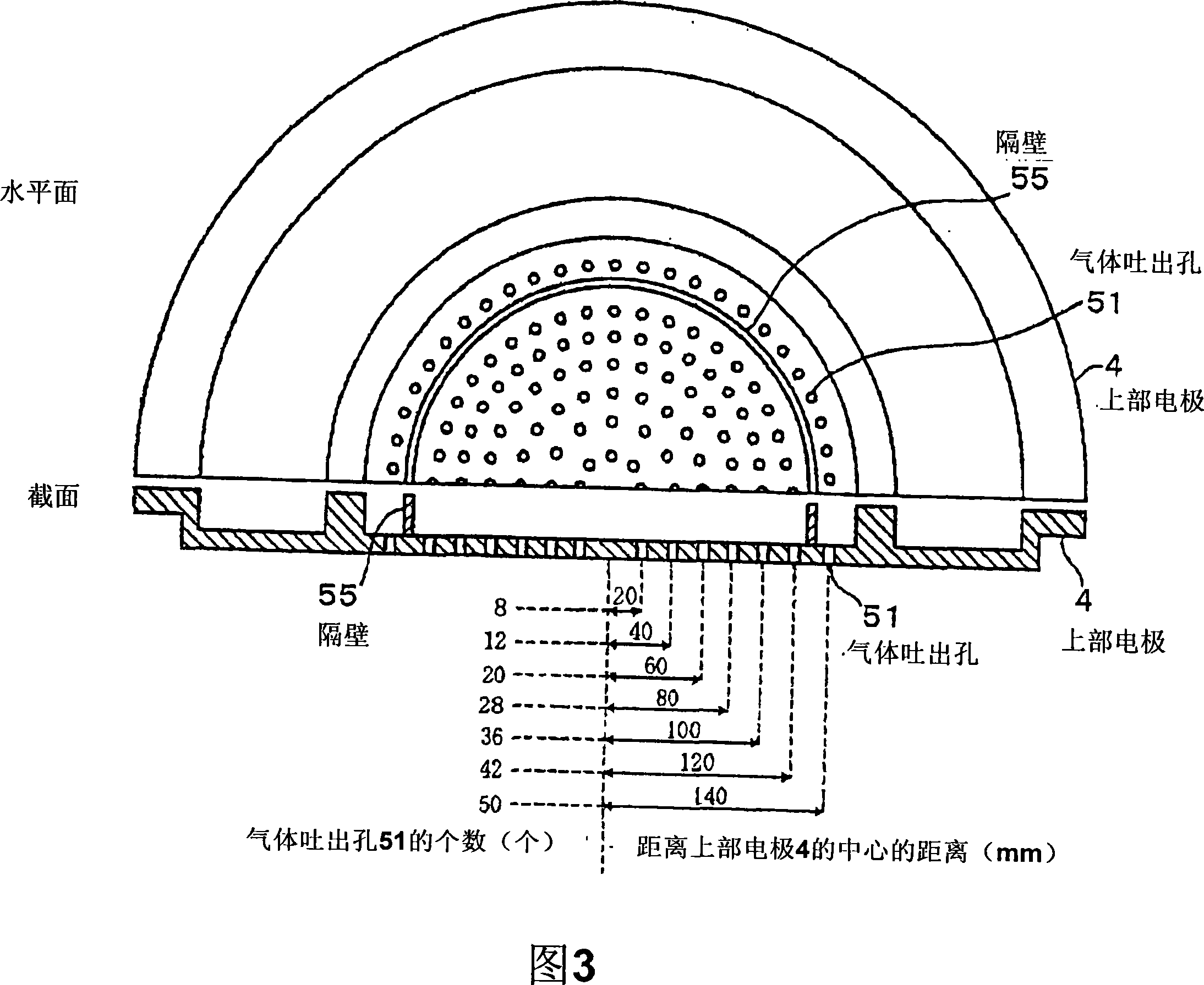
[0130] The radius of the outermost periphery of the gas discharge hole 51 communicating with the central region 53a is set to be 53%, 67% and 80% of the radius of the wafer W, respectively, and the distance L between the partition wall 55 and the upper electrode 4 is 90mm as shown in FIG. 5 , 110mm and 130mm.

[0131] In addition, the process conditions in the simulation test were set to the same conditions as in the above-mentioned Experimental Example 1 except ...

experiment example 3

[0157] (Experimental example 3: Verification of simulation test)

[0158] Next, an experiment was carried out to verify the results of the simulation test of Example 2. FIG. In the experiment, as outlined above, the same treatment as in Example 1 was performed, and the wafer W in the state shown in FIG. 4( b ) was etched. In addition, the same process conditions as Experimental Example 2 were set except for the conditions shown below.

[0159] (process conditions)

[0160] The distance L between the partition wall 55 and the center of the upper electrode 4 : to be explained separately

[0161] Processing pressure: 18.7Pa (140mTorr)

[0162] Process gas (gas source M): otherwise specified

[0163] Process gas (gas source A): otherwise specified


PUM


Abstract

The present invention is to provide a technique for uniformly processing a substrate surface in the process of processing a substrate by supplying a gas. The inside of a shower head having gas-jetting pores for supplying a gas to a substrate is partitioned into a center section from which a gas is supplied to the center portion of a substrate, and a peripheral section from which a gas is supplied to the peripheral portion of the substrate, and the same process gas is supplied to the substrate from these two sections at flow rates separately regulated. The distance from the center of the center section of the gas supply unit to the outermost gas-jetting pores in the center section is set 53% or more of the radius of the substrate. Moreover, an additional gas is further supplied to the peripheral portion of the substrate.

Description

technical field [0001] The present invention relates to a technique for supplying a gas to a substrate such as a semiconductor wafer for substrate processing, and more particularly to an apparatus for supplying the gas. Background technique [0002] In the manufacturing process of semiconductor equipment, a substrate is placed in a processing container, and a processing gas is supplied to the substrate in the form of a shower (shower) from a gas supply device called a gas shower head installed facing the substrate. , to perform processes such as etching and CVD on substrates such as semiconductor wafers (hereinafter referred to as wafers). [0003] On the other hand, with the miniaturization and high integration of patterns at the present stage, there is a process in which the pattern size in the substrate surface tends to become non-uniform. For example, in the process of forming the gate electrode of a transistor in a line shape by etching, if a resist mask is used to etc...

Claims


Application Information

Patent Timeline
Patent Type & Authority Applications(China)
IPC IPC(8): H01L21/00H01L21/02H01L21/311H01L21/67G05B19/04
CPCG03F7/2041G03F7/70691G03F9/7034H01L21/02312H01L21/02337H01L21/0274H01L21/2003
Inventor 益田法生
Owner TOKYO ELECTRON LTD
Why Eureka
Try Eureka