Method for making three-dimension electric casting micro structure

A manufacturing method and microstructure technology, applied in the direction of microstructure technology, microstructure devices, manufacturing microstructure devices, etc., can solve the problems of not processing micro switches, etc., and achieve small internal stress, good verticality of side walls, and structural strength high effect

Inactive Publication Date: 2008-03-26
DALIAN UNIV OF TECH
View PDF0 Cites 17 Cited by
  • Summary
  • Abstract
  • Description
  • Claims
  • Application Information

AI Technical Summary

Problems solved by technology

However, Document 2 only provides a processing and manufacturing plan for making a brush...

Method used


Image

  • Method for making three-dimension electric casting micro structure
  • Method for making three-dimension electric casting micro structure
  • Method for making three-dimension electric casting micro structure

Examples


Embodiment Construction

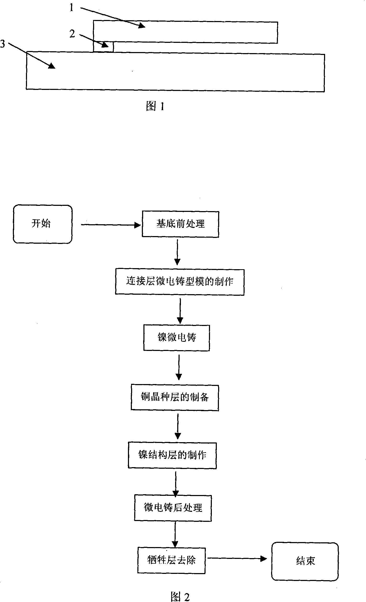
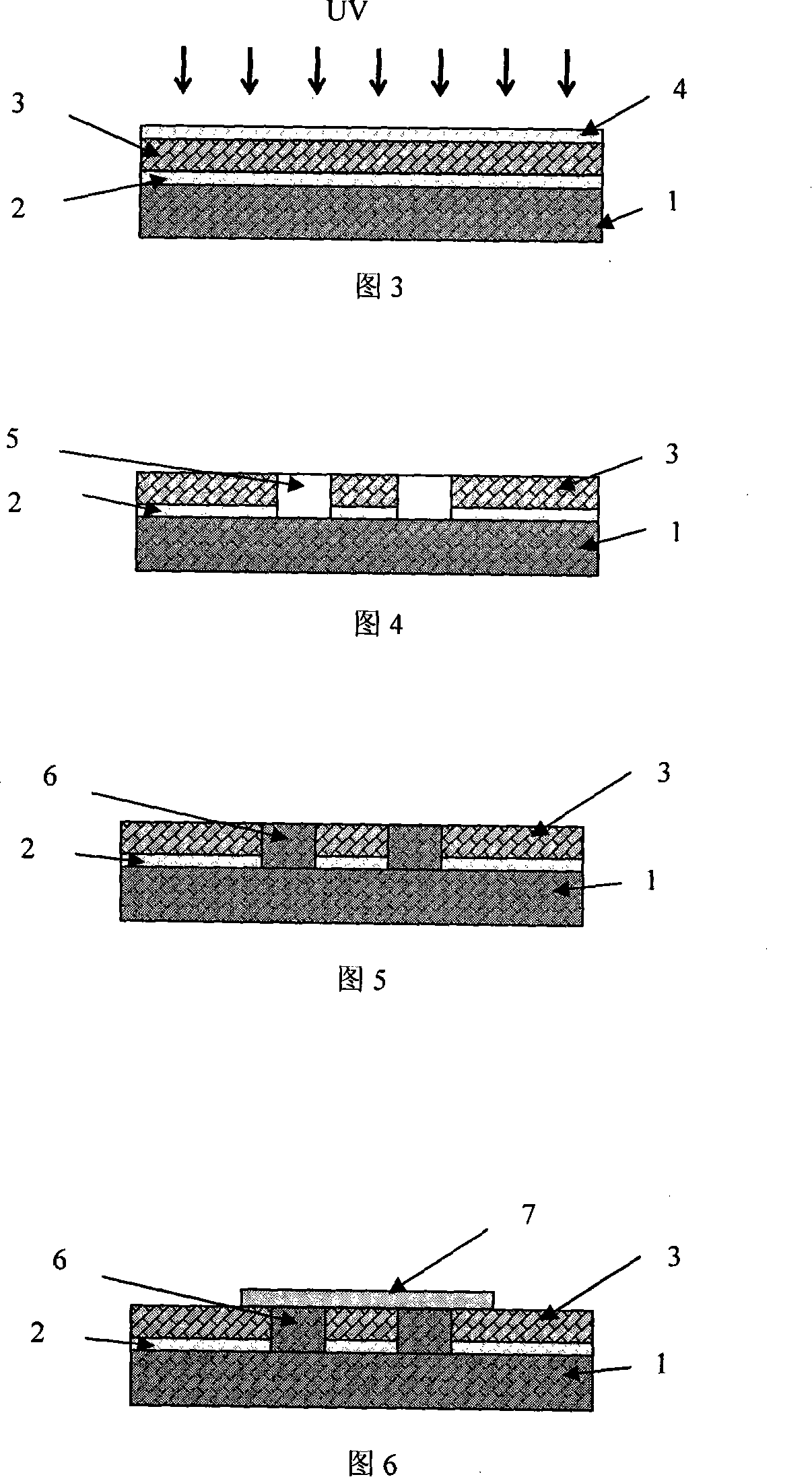
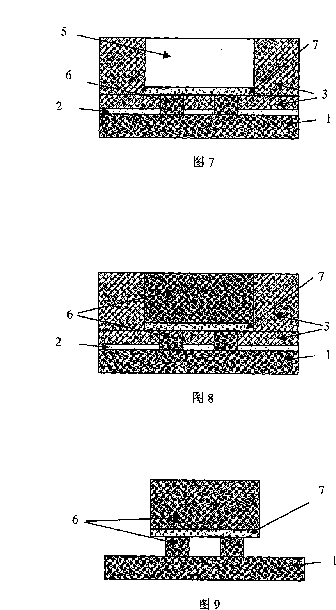
[0016] The specific implementation manners of the present invention will be described in detail below in conjunction with the accompanying drawings. For example: electroform a "cantilever" shape on a high-purity nickel substrate (53mm×63mm×2mm) after fine grinding and polishing (the size of the cantilever part 1 is 15mm×100um×300um, the connection layer 2 between the cantilever 1 and the substrate 3 Size is 100um * 100um * 50um, see the three-dimensional microstructure of accompanying drawing 1), it makes this structure according to the specific steps of flow chart 2 as follows:

[0017] 1. Substrate pretreatment The substrate material is high-purity nickel metal. The pretreatment of the nickel substrate is divided into two parts: mechanical processing pretreatment and surface cleaning. The mechanical processing pretreatment includes: milling, grinding, fine grinding, wire cutting and polishing. , The surface cleaning adopts the organic solvent degreasing method, and the organ...


PUM


Abstract

The present invention relates to micro electroformed metal devices, belongs to the field of micro manufacture technology, and is especially process of making 3D electroformed micro structure. The making process includes the steps of pre-treatment of the substrate, making micro electroforming mold for the connecting layer, micro electroforming, preparing copper crystal seed layer, making the nickel structure layer, post-treatment and eliminating the sacrificial layer. The process can make micro cantilever structure with firm binding and small interlayer stress, and the micro cantilever structure is applied as the key device of micro sensor and micro driver.

Description

technical field [0001] The invention belongs to the field of micro-manufacturing technology, and relates to metal base micro-electroforming metal devices. Background technique [0002] With the development of device miniaturization and MEMS technology, the three-dimensional cantilever microstructure has been widely used in the field of microsensors and microactuators as the core component of microsensors / actuators. Its processing method has attracted more and more attention of researchers. The fabrication of the existing three-dimensional cantilever microstructures is mainly realized by methods such as photolithography and micro-electroforming on silicon or glass substrates, such as pages 658-660 of the 5th issue of the journal "Journal of Xiamen University" in 2005 and the magazine "China Mechanical Engineering, Volume 16 Supplement, July 2005, Pages 252-254. The process flow of Document 1 is as follows: first, silicon dioxide is grown on a silicon substrate, a photolitho...

Claims


Application Information

Patent Timeline
IPC IPC(8): B81C1/00B81C5/00B81C99/00
Inventor 杜立群刘冲刘军山朱神渺刘文涛喻立川
Owner DALIAN UNIV OF TECH
Why Eureka
Try Eureka