Check patentability & draft patents in minutes with Patsnap Eureka AI!

Semiconductor encapsulation structure and its making process

A packaging process, semiconductor technology, applied in the direction of semiconductor/solid-state device manufacturing, semiconductor devices, semiconductor/solid-state device components, etc., can solve the problems of chip and chip carrier lamination, cracking, chip warping, etc., to improve the chip Warping or even cracking effect

Active Publication Date: 2008-03-26
ADVANCED SEMICON ENG INC
View PDF1 Cites 2 Cited by
  • Summary
  • Abstract
  • Description
  • Claims
  • Application Information

AI Technical Summary

Problems solved by technology

[0006] The object of the present invention is to provide a semiconductor packaging structure and its manufacturing process for tire pressure monitoring system, to overcome or at least improve the occurrence of delamination between the chip and the chip holder in the above-mentioned prior art, or chip warping or even cracking this question

Method used


Image

  • Semiconductor encapsulation structure and its making process
  • Semiconductor encapsulation structure and its making process
  • Semiconductor encapsulation structure and its making process

Examples


Embodiment Construction

[0014] Relevant detailed description and technical contents of the present invention are as follows now in conjunction with the accompanying drawings:

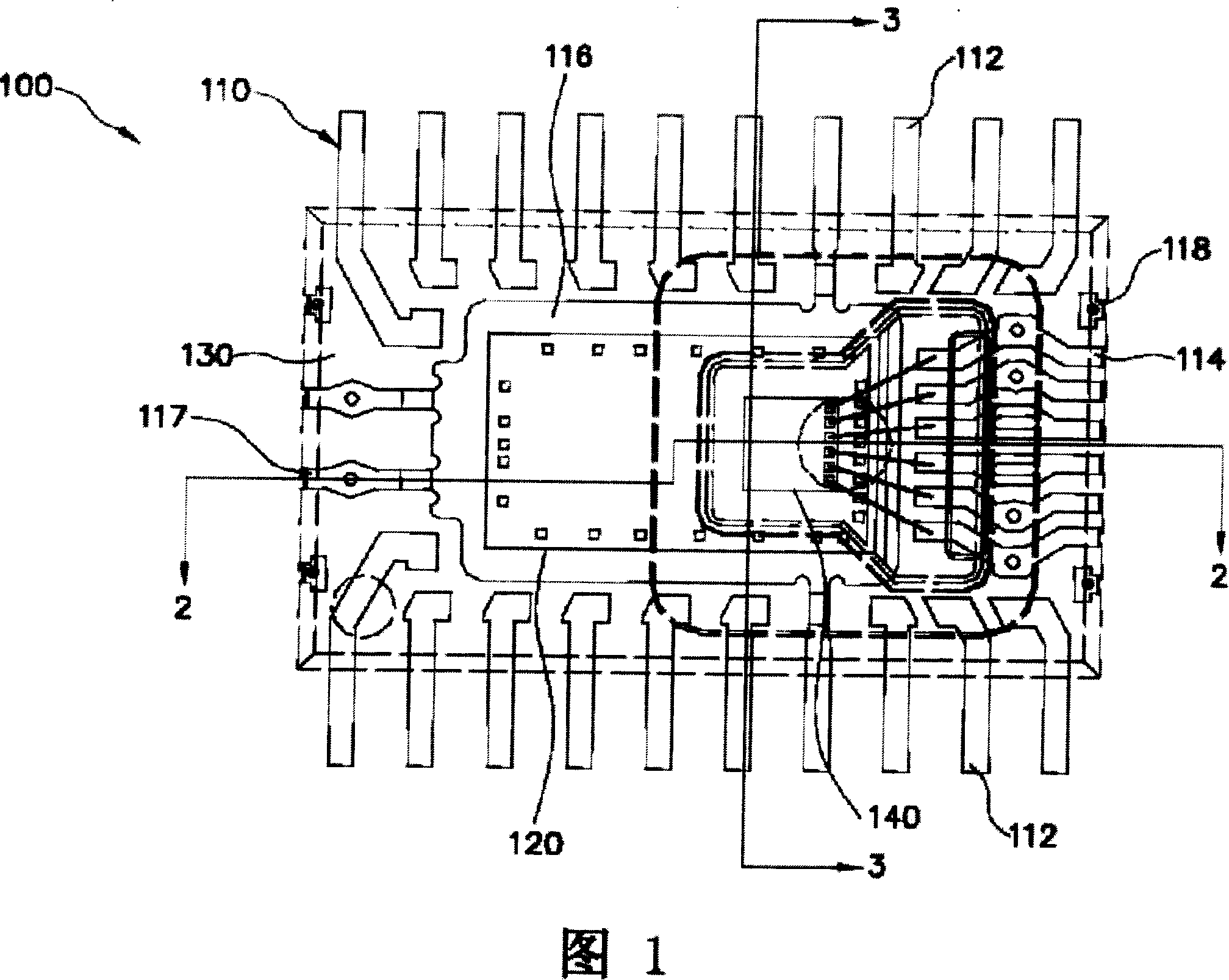
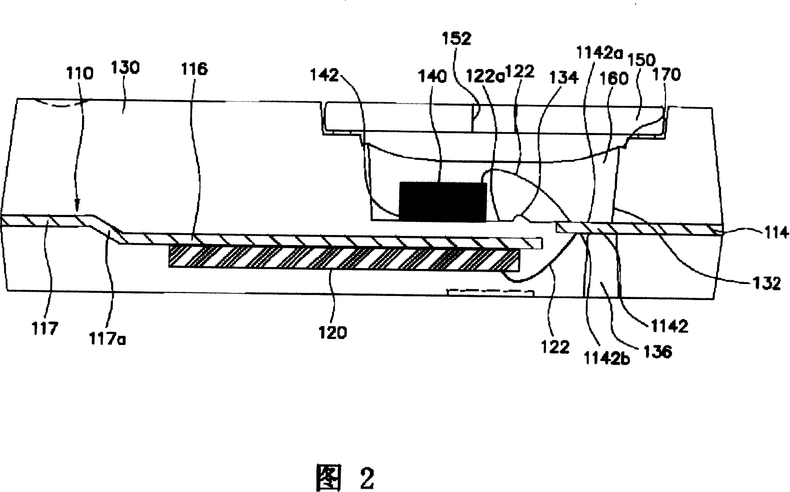
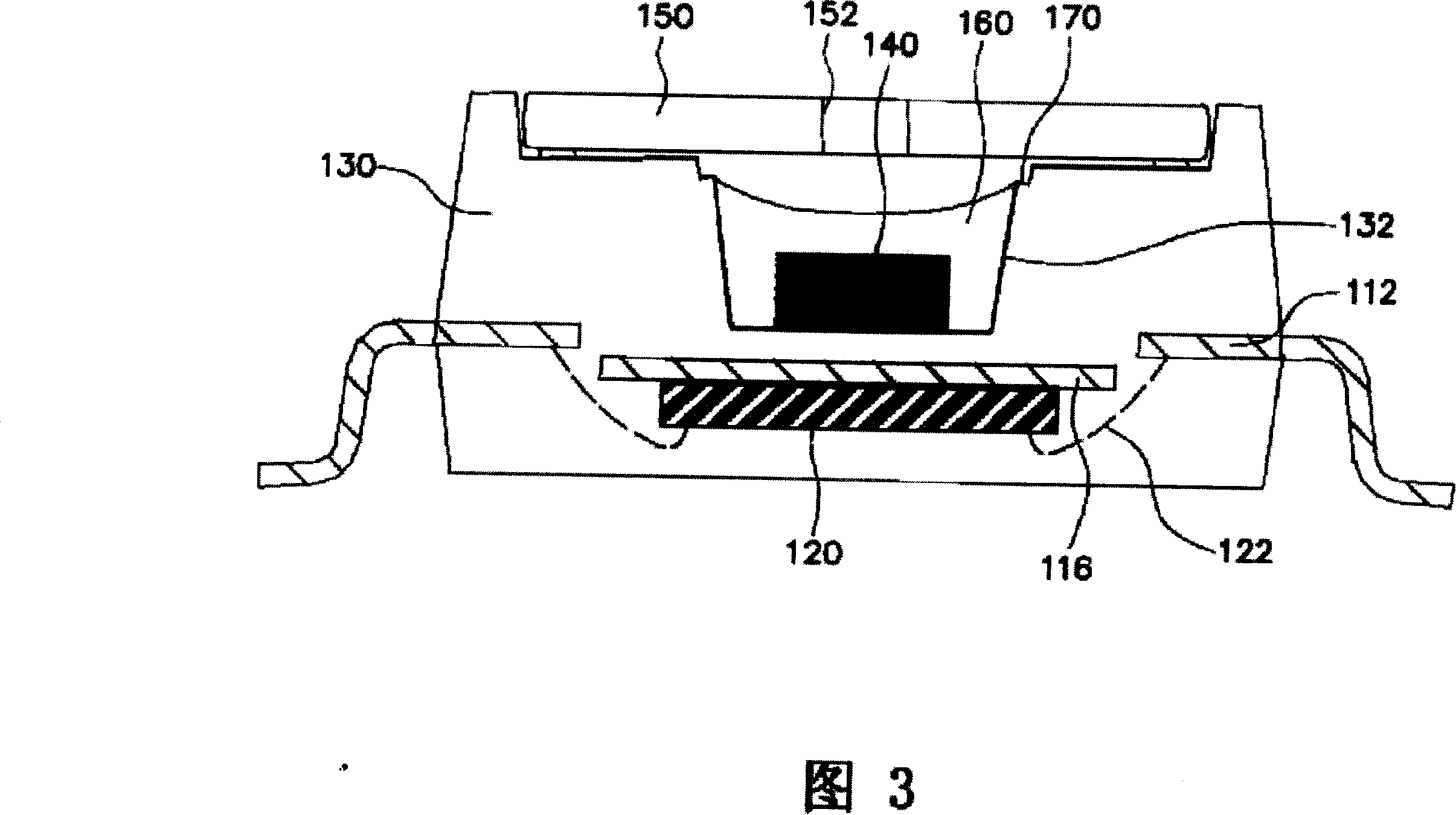
[0015] 1-3 illustrate a semiconductor package structure 100 according to a preferred embodiment of the present invention. FIG. 1 is a top view of the semiconductor package structure 100 . Fig. 2 is a cross-sectional view taken along section line 2-2 in Fig. 1 . Fig. 3 is a sectional view taken along section line 3-3 in Fig. 1 . As shown in FIG. 1 , the semiconductor package structure 100 mainly includes a lead frame 110, a first semiconductor chip 120 wrapped in a first encapsulant 130 (the first encapsulant 130 has a recess 132 for containing Put a second semiconductor chip 140, and a cover 150 (see Fig. 2 and Fig. 3 ) that is located on the recess 132 of the first encapsulant 130. For example, the first semiconductor chip 120 can be a Discrete components, an integrated circuit or a control chip, and the second semiconduct...


PUM


Abstract

This invention relates to a semiconductor package structure including a lead frame, a first semiconductor chip wrapped in a first sealing colloid (such as ASIC), which includes a concave for containing a second semiconductor chip ( such as a pressure sensing chip) and a cover set on the concave of the first sealing colloid, a part of which is formed between the second semiconductor chip and the loader of the chip so that the second semiconductor chip is not set on the snug of the chip but on the place of the first sealing colloid.

Description

technical field [0001] The present invention relates to a semiconductor package structure, in particular to a semiconductor package structure with a plurality of semiconductor chips. Background technique [0002] With the ever-increasing demand for miniaturization and high operating speed, a semiconductor package structure with a plurality of semiconductor chips (ie, a multi-chip package structure) is becoming more and more attractive in many electronic devices. Multi-chip package construction minimizes the limitation on system operating speed caused by long printed circuit board connection lines by combining processor, memory and logic chips in a single package construction. In addition, the multi-chip package structure can reduce the length of the connection lines between chips and reduce signal delay and access time. [0003] However, in some applications (such as a tire pressure monitoring system used to monitor automobile tire pressure), it is desirable to integrate a ...

Claims


Application Information

Patent Timeline
IPC IPC(8): H01L25/00H01L23/31H01L23/488H01L21/50H01L21/56H01L21/60B81B7/00B81C3/00
CPCH01L2224/48091H01L2224/48247
Inventor 郑大训李锡元朴善裴
Owner ADVANCED SEMICON ENG INC
Features
  • R&D
  • Intellectual Property
  • Life Sciences
  • Materials
  • Tech Scout
  • Unparalleled Data Quality
  • Higher Quality Content
  • 60% Fewer Hallucinations
Learn More