Mobile phone antenna medium substrates with anti-symmetric structure left hand material

An asymmetric structure, mobile phone antenna technology, applied in the direction of antenna, electrical components, etc., can solve the problems of complexity, poor directivity, conductor and dielectric loss, etc.

Inactive Publication Date: 2008-04-16
NORTHWESTERN POLYTECHNICAL UNIV
View PDF0 Cites 44 Cited by
  • Summary
  • Abstract
  • Description
  • Claims
  • Application Information

AI Technical Summary

Problems solved by technology

For example, the mobile phone uses two channels of 900MHz (GSM specification) and 1800MHz (DCS specification). For this reason, the antenna used on the mobile phone has also been changed from a single-frequency antenna to a dual-frequency antenna that can support a dual-frequency system. The built-in flat-panel antenna is mostly used in the multi-band antenna. Considering the structural characteristics of the antenna itself, the dual-band antenna has disadvantages such as low gain, poor directivity, conductor and dielectric loss, and low radiation efficiency.
Usually, using one device or material can only simply improve the performance of the antenna in a certain frequency band, but it becomes more complicated to improve the performance of the antenna in dual frequency bands at the same time

Method used


Image

  • Mobile phone antenna medium substrates with anti-symmetric structure left hand material
  • Mobile phone antenna medium substrates with anti-symmetric structure left hand material
  • Mobile phone antenna medium substrates with anti-symmetric structure left hand material

Examples


Embodiment 1

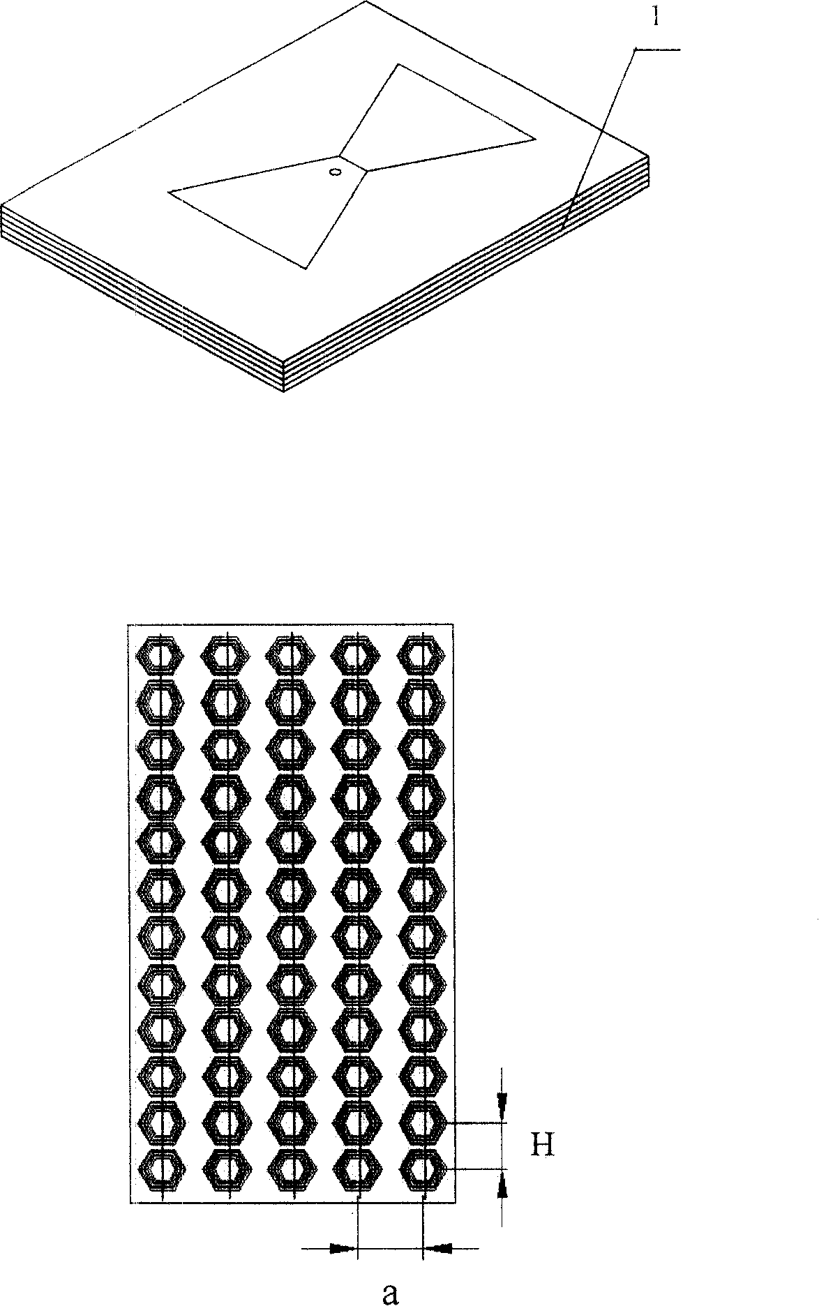
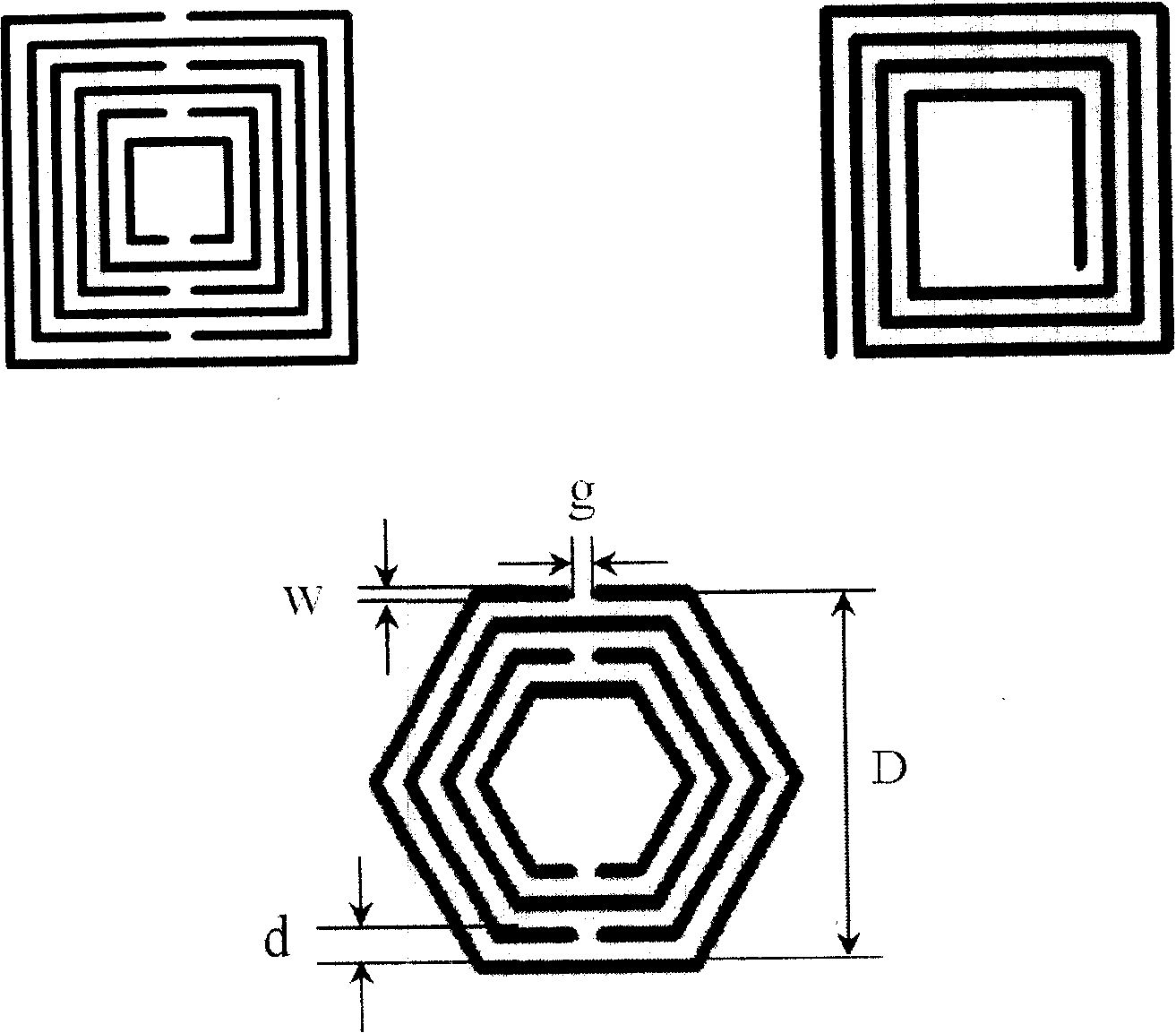
[0014] The left-hand material dielectric substrate 1 is produced by circuit board etching technology, and its specific preparation process is as described in the implementation mode. The left-hand material structural unit used in this embodiment is a metal copper hexagonal opening resonance four-ring and a metal copper wire, wherein the metal copper It can be replaced by metals such as gold, silver, zinc, and tin. On one side of a polytetrafluoroethylene dielectric substrate (ε=2.6) with a thickness of 0.25-1.20mm, etch an open resonant four-ring, and its geometric size is: the diameter of the inscribed circle of the outermost ring D=5.50mm, adjacent Ring spacing d=0.80mm, opening g=0.30mm, line width c=0.50mm, thickness 0.02mm; metal line etched on the other side, its geometric dimensions: line width c=0.50~0.90mm, thickness 0.02mm, The distance between the upper and lower ends of the metal line and the edge of the substrate is 1 = 2.50mm; the row spacing H 0 = 7.00mm, colum...

Embodiment 2

[0016] The left-hand material dielectric substrate 1 is produced by circuit board etching technology, and its specific preparation process is as described in the implementation mode. The left-hand material structural unit used in this embodiment is metal copper hexagonal opening resonant six rings and metal copper wire, wherein the metal copper It can be replaced by metals such as gold, silver, zinc, and tin. On one side of a polytetrafluoroethylene dielectric substrate (ε=2.6) with a thickness of 0.25-1.20mm, etch an open resonant six-ring, and its geometric dimensions are: the diameter of the inscribed circle of the outermost ring is D=5.20mm, adjacent Ring spacing d = 0.40mm, opening g = 0.25mm, line width c = 0.30mm, thickness 0.02mm; the other side etched metal lines, its geometric dimensions: line width c = 0.50 ~ 0.90mm, thickness 0.02mm, The distance between the upper and lower ends of the metal line and the edge of the substrate is 1 = 2.50mm; the row spacing H 0 =6....

Embodiment 3

[0018] The left-hand material dielectric substrate 1 is produced by circuit board etching technology, and its specific preparation process is as described in the implementation mode. The left-hand material structural unit used in this embodiment is metal copper hexagonal opening resonant six rings and metal copper wire, wherein the metal copper It can be replaced by metals such as gold, silver, zinc, and tin. On one side of a polytetrafluoroethylene dielectric substrate (ε=2.6) with a thickness of 0.25-1.20mm, etch an open resonant six-ring, and its geometric size is: the diameter of the inscribed circle of the outermost ring is D=4.85mm, adjacent Ring spacing d = 0.25mm, opening g = 0.10mm, line width c = 0.15mm, thickness 0.02mm; the other side is etched metal line, its geometric dimensions: line width c = 0.50 ~ 0.90mm, thickness 0.02mm, The distance between the upper and lower ends of the metal line and the edge of the substrate is 1 = 2.50mm; the row spacing H 0 =5.70mm,...


PUM


Abstract

The present invention relates to a cellphone antenna medium placode, in particular to a double frequency cellphone antenna medium placode with asymmetric structure left hand material, wherein, the left hand material has double left hand transmission band which is made by introducing the metal resonant ring of non-equal line space. The present invention uses the double left hand band with the asymmetric structure left hand material to realize effective amplification for the evanescent wave in electromagnetic wave in two power frequency sections of low frequency 900MHz and high frequency 1800MHz in cellphone antenna, and the evanescent wave participates in the radiation and receiving work of the antenna to signal, thereby improving radiation efficiency of the cellphone antenna and gains of the cellphone antenna.

Description

technical field [0001] The invention relates to a mobile phone antenna dielectric substrate, in particular to an asymmetric structure left-handed material dielectric substrate with double left-handed passbands. The mobile phone antenna made of this substrate can increase sensitivity and performance in dual frequency bands respectively. Background technique [0002] Left-handed materials (LHMs, Left-handed Metamaterials) are peculiar materials whose permittivity and permeability are negative at the same time in a certain electromagnetic wave response frequency band, because the electromagnetic wave electric field vector, magnetic field vector and wave propagation direction propagating in it Satisfy the left-hand rule and get the name. Subsequent studies have found that periodically arranged metal split resonator rings (SRRs) and rods can achieve negative permittivity and negative magnetic permeability in a specific frequency band, and a transmission passband, that is, a left-...

Claims


Application Information

Patent Timeline
Patent Type & Authority Applications(China)
IPC IPC(8): H01Q15/00
Inventor 赵晓鹏宋娟
Owner NORTHWESTERN POLYTECHNICAL UNIV
Why Eureka
Try Eureka