Plane indium and gallium infrared focusing plane detector and its making method

An infrared focal plane, indium gallium arsenic technology, applied in the direction of semiconductor devices, final product manufacturing, sustainable manufacturing/processing, etc., can solve the problems of pn junction difficulty, p electrode system process complexity, photosensitive element expansion, etc., to achieve Enhanced thermal stability, easy process, precise control effect

Inactive Publication Date: 2008-04-30
SHANGHAI INST OF TECHNICAL PHYSICS - CHINESE ACAD OF SCI
View PDF0 Cites 9 Cited by
  • Summary
  • Abstract
  • Description
  • Claims
  • Application Information

AI Technical Summary

Problems solved by technology

[0003] Based on the problems existing in the above-mentioned existing devices, the purpose of the present invention is to propose a planar indium gallium arsenic infrared focal plane d...

Method used


Image

  • Plane indium and gallium infrared focusing plane detector and its making method
  • Plane indium and gallium infrared focusing plane detector and its making method

Examples


Embodiment Construction

[0023] Below in conjunction with accompanying drawing and embodiment the specific embodiment of the present invention is described in further detail:

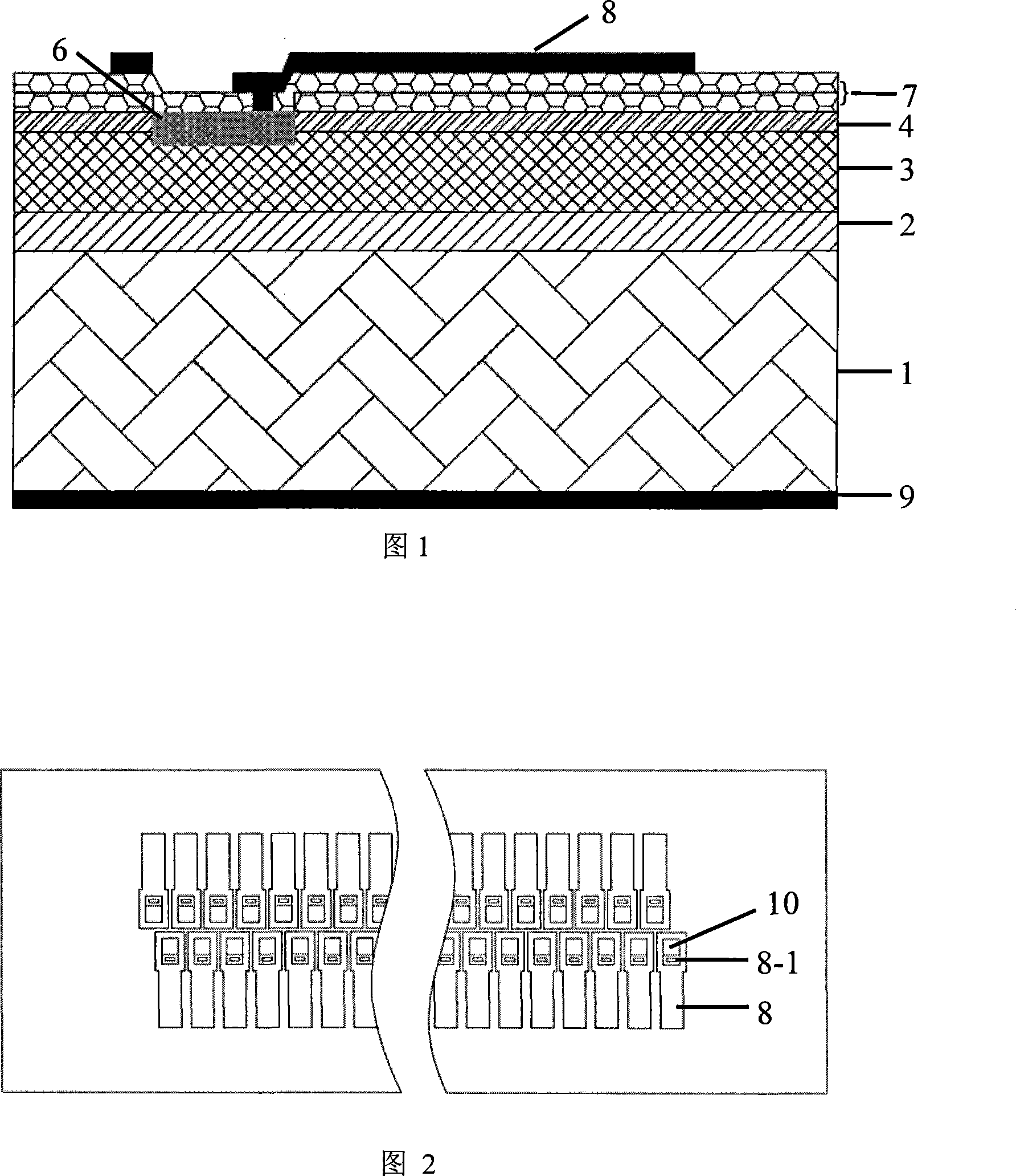
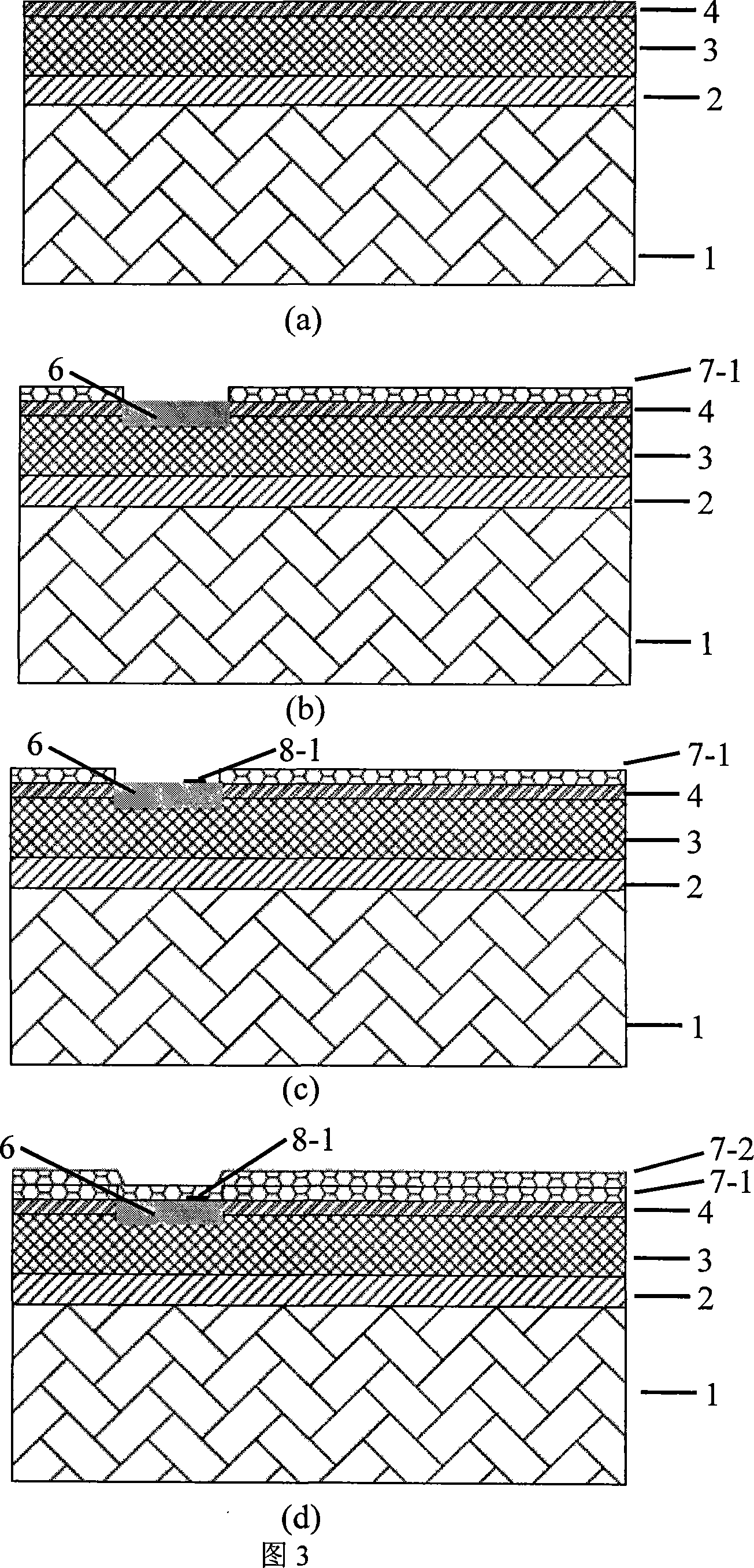
[0024] As shown in Figure 3a, the structure of the epitaxial wafer used in this embodiment is: n-type InP substrate 1 with a thickness of 650 μm, and a carrier concentration of 3-4×10 18 cm -3 ; Use MOCVD technology to sequentially grow n-type InP layer 2 with a thickness of 0.5 μm on the substrate 1, with a carrier concentration of 2-3×10 18 cm -3 ; In with a thickness of 2.5 μm 0.53 Ga 0.47 As intrinsic absorption layer 3, carrier concentration 5-6×10 16 cm -3 ; An n-type InP cap layer 4 with a thickness of 1 μm and a carrier concentration greater than 5×10 16 cm -3 . Then ultrasonically clean the epitaxial wafer with chloroform, ether, acetone, and ethanol in sequence, and dry it with nitrogen gas; photolithography of positive resist (thick resist), and drying at 65°C for 20 minutes after photolithography;

[0025] ...


PUM


Abstract

The invention discloses a flat type InGaAs infrared focal plane device, which includes a flat type PN junction formed by Zn diffusion on an epitaxial wafer. The invention is characterized in that: a thickened Cr/Au ring electrode is positioned around the upper part of the Zn diffusion area and the limitation on a photosensor element is realized by the Au layer reflection of incident lights. The shape of the thickened electrode is decided by a photoetching graph, so the effective photosensor element area can be controlled precisely. The preparation method of the device is characterized in that: before heat treatment, generate SiO2 passive film to prevent Zn from out diffusion in the heat treatment course, improve PN junction thermal stability, and realize device surface passivation and light antireflection by controlling the thickness of SiO2 film. p electrode adopts single Au layer, which simplifies p electrode growth process and is important to process stability and device evenness. The Au and the InP have better adhesiveness. And the thermal annealing course under the protection of SiO2 layer can realize good ohmic contact with Au/Zn/Au.

Description

technical field [0001] The invention relates to a planar indium gallium arsenic infrared focal plane detector, in particular to a device structure and a preparation method. Background technique [0002] The planar InGaAs detector is the mainstream structure of the InGaAs detector, which mainly adopts Zn diffusion method to achieve p-type doping in n-InP / InGaAs / n-InP epitaxial materials to prepare the pn junction region of the photosensitive element . The device obtained by this method has small dark current, high detection rate and long life, and is suitable for application in the field of aerial remote sensing. But it has some unavoidable disadvantages: 1) The thermal stability of the pn junction is poor, because the diffusion coefficient of the Zn element in InP is large, which makes it easy to diffuse outwards in the subsequent heat treatment and cause the pn junction to collapse. Stability deteriorates. 2) The photosensitive element is enlarged, and the longer minorit...

Claims


Application Information

Patent Timeline
IPC IPC(8): H01L31/103H01L31/0224H01L31/18
CPCY02P70/50
Inventor 吴小利唐恒敬张可峰李雪龚海梅
Owner SHANGHAI INST OF TECHNICAL PHYSICS - CHINESE ACAD OF SCI
Why Eureka
Try Eureka