
A white light organic EL part consisting of RGB and its making method

An electroluminescent device and organic technology, applied in electroluminescent light sources, chemical instruments and methods, electrical components and other directions, can solve the problems of complex process, difficulty in improving resolution, difficulty in precise alignment, etc., and achieve a reasonable and simple preparation method. , fast response, wide viewing angle effect

Inactive Publication Date: 2008-04-30
UNIV OF ELECTRONICS SCI & TECH OF CHINA
View PDF0 Cites 23 Cited by
  • Summary
  • Abstract
  • Description
  • Claims
  • Application Information

AI Technical Summary

Problems solved by technology

[0008] Among the above methods, the process in the preparation process of method 4 is extremely complicated
Although full-color display devices based on method 1 have been released, precise pixel preparation requires high-quality evaporation templates, which brings difficulties in precise alignment and makes it difficult to improve resolution

Method used


Image

  • A white light organic EL part consisting of RGB and its making method
  • A white light organic EL part consisting of RGB and its making method
  • A white light organic EL part consisting of RGB and its making method

Examples


Embodiment 1

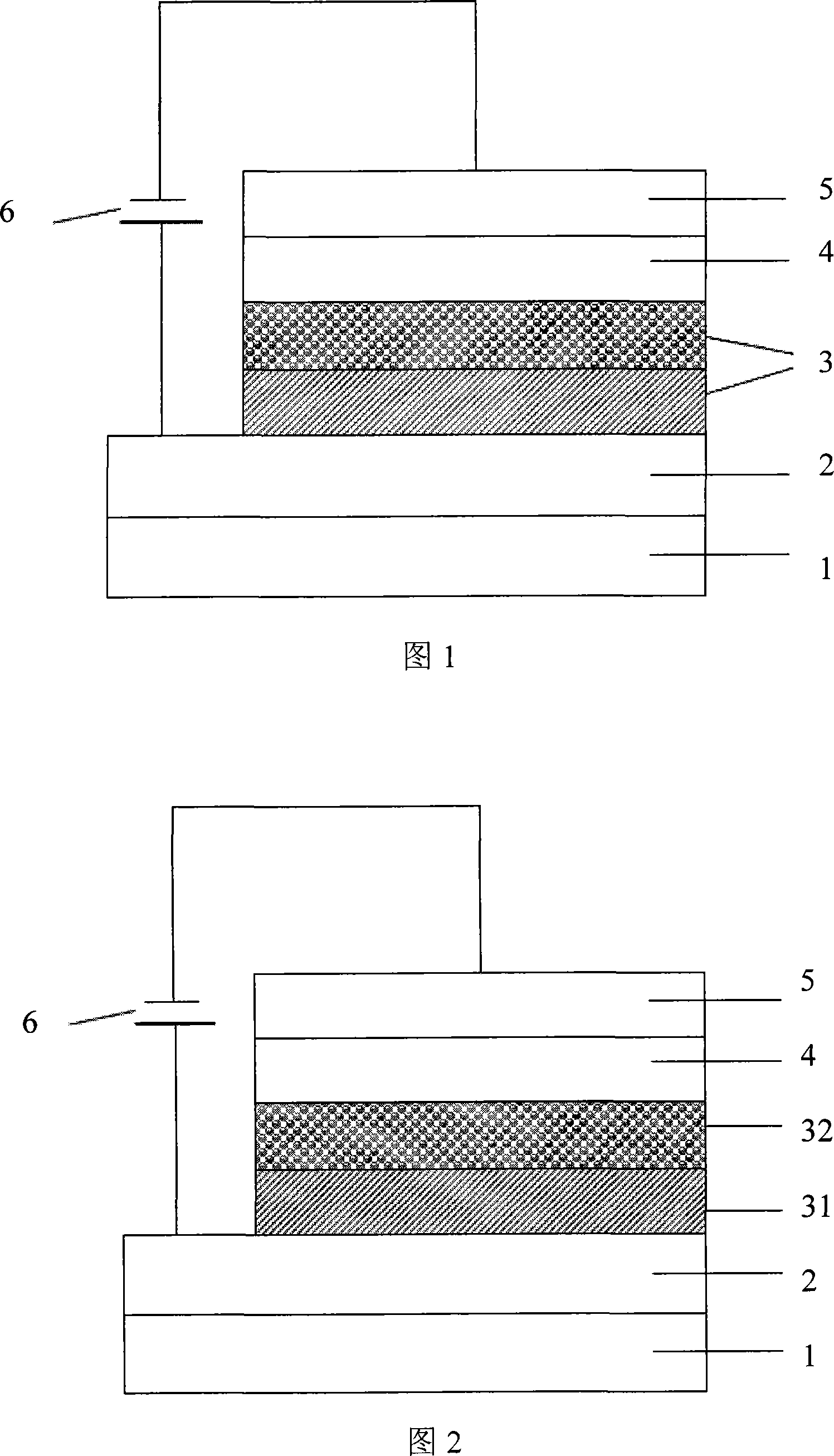
[0089] As shown in FIG. 2 , the light emitting layer 3 in the structure of the device includes a hole transport layer also serving as a blue light emitting layer 31 , a green light emitting layer also serving as a red light emitting layer 32 , and a hole blocking layer also serving as an electron transport layer 4 .

[0090] The fluorescent material emitting blue light of the device is NPB, the fluorescent material emitting green light and the phosphorescent dye emitting red light are Alq 3 :(nazo) 2 Ir(Fppz), the hole blocking layer doubles as the electron transport material BCP, and the cathode layer uses Mg:Ag alloy. The entire device structure is described as:

[0091] Glass substrate / ITO / NPB(50nm) / Alq 3 :(nazo) 2 Ir(Fppz)(40nm) / BCP(20nm) / Mg:Ag(100nm)

[0092] The preparation method is as follows:

[0093] ①Use detergent, ethanol solution and deionized water to ultrasonically clean the transparent conductive substrate ITO glass, and dry it with dry nitrogen after clea...

Embodiment 2

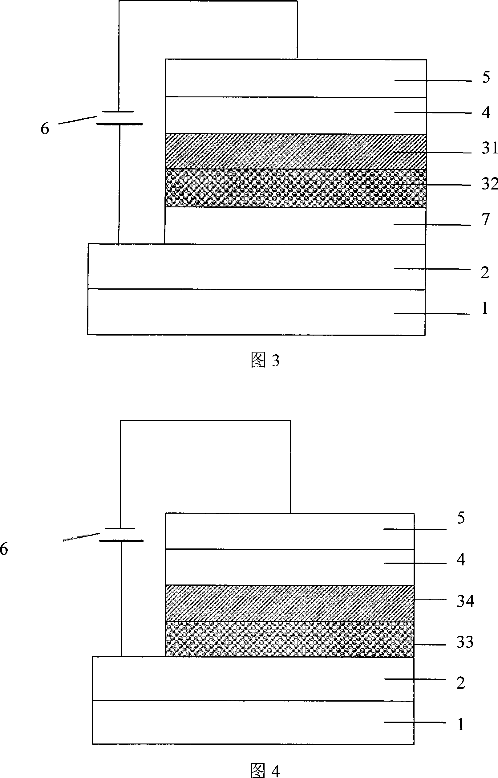
[0100] As shown in Figure 3, the light emitting layer 3 in the structure of the device includes a hole transport layer 7, the hole transport layer doubles as a blue light emitting layer 31, the green light emitting layer doubles as a red light emitting layer 32, and the hole blocking layer doubles as an electron transport layer 4.

[0101] The fluorescent material emitting blue light of the device is NPB, the fluorescent material emitting green light and the phosphorescent dye emitting red light are Alq 3 :(nazo) 2 Ir(Fppz), the hole transport layer material is NPB, the hole blocking layer doubles as the electron transport material BCP, and the cathode layer uses Mg:Ag alloy. The entire device structure is described as:

[0102] Glass substrate / ITO / NPB(40nm) / Alq 3 :(nazo) 2 Ir(Fppz)(40nm) / NPB(10nm) / BCP(20nm) / Mg:Ag(100nm)

[0103] The fabrication process of the device is similar to that of Example 1.

Embodiment 3

[0105] As shown in FIG. 4 , the light-emitting layer 3 in the structure of the device includes a hole-transport layer that doubles as a blue light-emitting layer and a red light-emitting layer 33 , a green light-emitting layer 34 , and a hole-blocking layer that doubles as an electron-transport layer 4 .

[0106] The fluorescent material emitting blue light and the phosphorescent dye emitting red light of the device are NPB: (nazo) 2 Ir(Fppz), the fluorescent material that emits green light is Alq 3 , The hole blocking layer doubles as the electron transport material BCP, and the cathode layer uses Mg:Ag alloy. The entire device structure is described as:

[0107] Glass substrate / ITO / NPB:(nazo) 2 Ir(Fppz)(50nm) / Alq 3 (40nm) / BCP(20nm) / Mg:Ag(100nm)

[0108] The fabrication process of the device is similar to that of Example 1.


PUM

PropertyMeasurementUnit
thicknessaaaaaaaaaa

Abstract

The invention discloses a white light organic electrofluorescence device which comprises RGB and includes an underlay, an anode layer and a cathode layer. An electrode is positioned on the surface of the underlay. An organic function layer equipped between the anode layer and the cathode layer includes a luminous layer at least and sends out white light under external power drive. The luminous layer comprises of RGB luminescent materials. A composite material layer consisting of blue and light fluorescent material, red, green and blue phosphorescence material and main host material sends out efficient white light under the external power drive. The invention adopts the method of doped phosphorescence material, adjusts proper doped concentration, and prepares high-performance white light and other color organic electrofluorescence device by utilizing the main and the object materials with luminescence principle.

Description

technical field [0001] The invention relates to the technical field of organic electroluminescence in electronic components, in particular to a white light organic electroluminescence device composed of RGB and a preparation method thereof. Background technique [0002] Organic electroluminescent technology (OLED) has become a research hotspot. Because its development provides technical support and guarantee for micro-display or large-area information display, and has significant advantages: self-illumination, low power consumption, high and low temperature resistance, full curing, wide viewing angle, rich colors, no need for backlight, high Response speed (up to 1000 times that of LCD), while its manufacturing cost is much lower than that of LCD with the same performance. [0003] Full-color, large-area, high-information flat-panel displays are one of the most important goals for the development of OLEDs. With the maturity of monochromatic light-emitting displays, the res...

Claims


Application Information

Patent Timeline
Patent Type & Authority Applications(China)
IPC IPC(8): H05B33/12H05B33/14H05B33/26C09K11/06
CPCY02B20/181Y02B20/00
Inventor 蒋亚东李璐于军胜王军
Owner UNIV OF ELECTRONICS SCI & TECH OF CHINA
Learn More