InAlGaN/GaN PIN photoelectric detector without strain

A photodetector, strain-free technology, applied in the field of photodetectors

Inactive Publication Date: 2008-05-28
XIAMEN UNIV
View PDF0 Cites 22 Cited by
  • Summary
  • Abstract
  • Description
  • Claims
  • Application Information

AI Technical Summary

Problems solved by technology

[0004] The purpose of the present invention is to provide a strain-free InAlGa

Method used


Image

  • InAlGaN/GaN PIN photoelectric detector without strain

Examples


Embodiment Construction

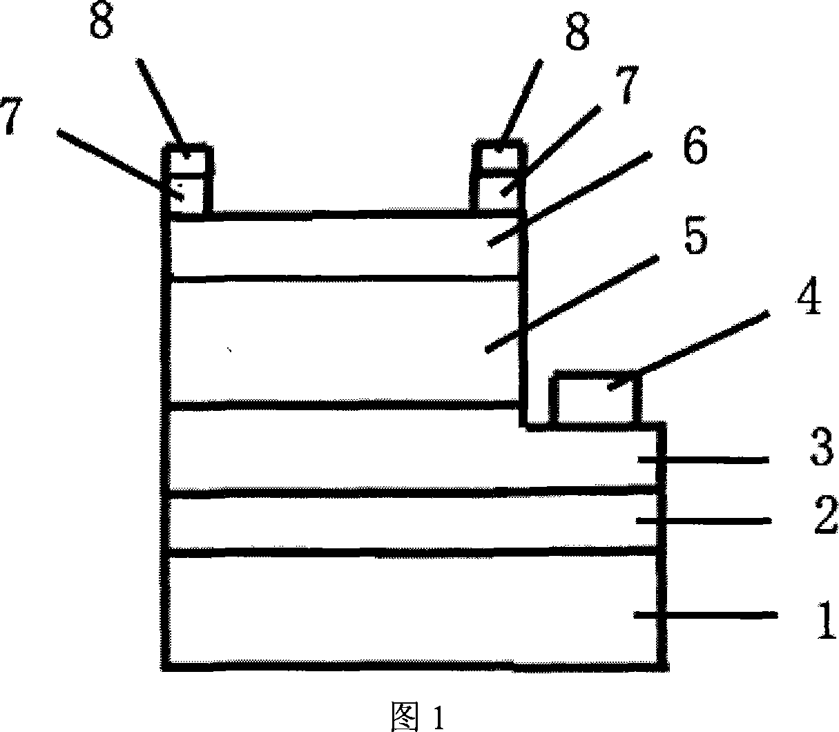
[0014] Referring to Fig. 1, the present invention is provided with sapphire (Al 2 o 3 ) substrate 1, GaN buffer layer 2, n-GaN layer 3, i-InAlGaN photosensitive layer 5, p-InAlGaN layer 6 and p-GaN top layer 7, from bottom to top GaN buffer layer 2, n-GaN layer 3, i -InAlGaN photosensitive layer 5, p-InAlN layer 6 and p-GaN top layer 7 are arranged on sapphire (Al 2 o 3 ) on the substrate 1, a p-electrode 8 is provided on the p-GaN top layer 7, and an n-electrode 4 is provided on the n-GaN layer 3.

[0015] The thickness of the GaN buffer layer 2 is 1-3 μm, the thickness of the n-GaN layer 3 is 1-3 μm, the thickness of the i-InAlGaN photosensitive layer 5 is 100-400 nm, the thickness of the p-InAlN layer 6 is 50-400 nm, and the p- The GaN top layer 7 has a thickness of 5-50 nm.

[0016] The p electrode 8 adopts a Ni / Au metal electrode, and the thickness of the Ni / Au metal electrode is (5-20) nm / (5-20) nm; the n-electrode 4 adopts a Cr / Al / Au metal electrode, and the Cr / Al / A...


PUM

PropertyMeasurementUnit
Thicknessaaaaaaaaaa
Thicknessaaaaaaaaaa
Thicknessaaaaaaaaaa

Abstract

An unstrained InAlGaN/GaN PIN photodetector relates to a photodetector, in particular to an InAlGaN/GaN PIN photodetector which can convert light signals into electrical signals. The invention provides an unstrained InAlGaN/GaN PIN photodetector. The invention is provided with sapphire (Al2O3) substrates, a GaN buffer layer, a n-GaN layer, an i-InAlGaN photosensitive layer, a p-InAlN layer and a p-GaN top layer. The GaN buffer layer, the n-GaN layer, the i-InAlGaN photosensitive layer and the p-GaN top layer are orderly arranged on the sapphire (Al2O3) substrates from lower to top. A p-electrode is arranged on the p-GaN top layer, and a n-electrode is arranged on the n-GaN layer.

Description

technical field [0001] The invention relates to a photodetector, in particular to an indium aluminum gallium nitride / gallium nitride (InAlGaN / GaN) PIN photodetector for converting optical signals into electrical signals. Background technique [0002] GaN-based materials (that is, III-V nitrides mainly include GaN, AlN, InN and their ternary and quaternary alloy solid solutions) have wide direct bandgap, strong chemical bonds, high temperature resistance, corrosion resistance, high breakdown electric field, High electron saturation rate and other characteristics are ideal materials for manufacturing short-wavelength high-brightness light-emitting devices, semiconductor lasers, ultraviolet light detectors, and high-temperature, high-frequency microelectronics. And because GaN-based ternary alloys and quaternary alloys have continuously adjustable band gaps, their corresponding direct bandgap bands cover from visible light to ultraviolet light. This makes GaN-based application...

Claims


Application Information

Patent Timeline
IPC IPC(8): H01L31/105H01L31/0304
Inventor 刘宝林张保平毛明华
Owner XIAMEN UNIV
Why Eureka
Try Eureka