Reaction cavity lining and reaction cavity including the same

A reaction chamber and lining technology, applied in the direction of gaseous chemical plating, coating, electrical components, etc., can solve the problems of inconsistent gas flow, uneven internal pressure, uneven distribution of plasma, etc., to achieve uniform gas distribution, Effect of Uniform Etch Rate

Active Publication Date: 2008-06-11
BEIJING NAURA MICROELECTRONICS EQUIP CO LTD
View PDF0 Cites 27 Cited by
  • Summary
  • Abstract
  • Description
  • Claims
  • Application Information

AI Technical Summary

Problems solved by technology

[0008] In order not to affect the process, the cross-sectional area of ​​the exhaust port 6 is generally relatively large. The distance between the reaction chamber and the exhaust port is different, and the gas flow is inconsistent, resulting in uneven internal pressure and uneven distribution of plasma, which affects the etching process results.

Method used


Image

  • Reaction cavity lining and reaction cavity including the same
  • Reaction cavity lining and reaction cavity including the same

Examples


Embodiment Construction

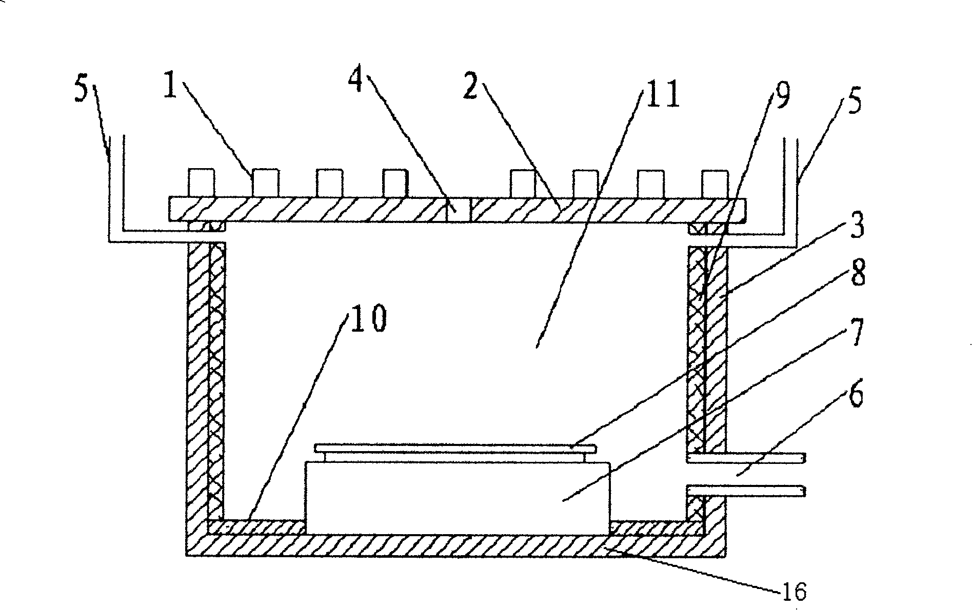
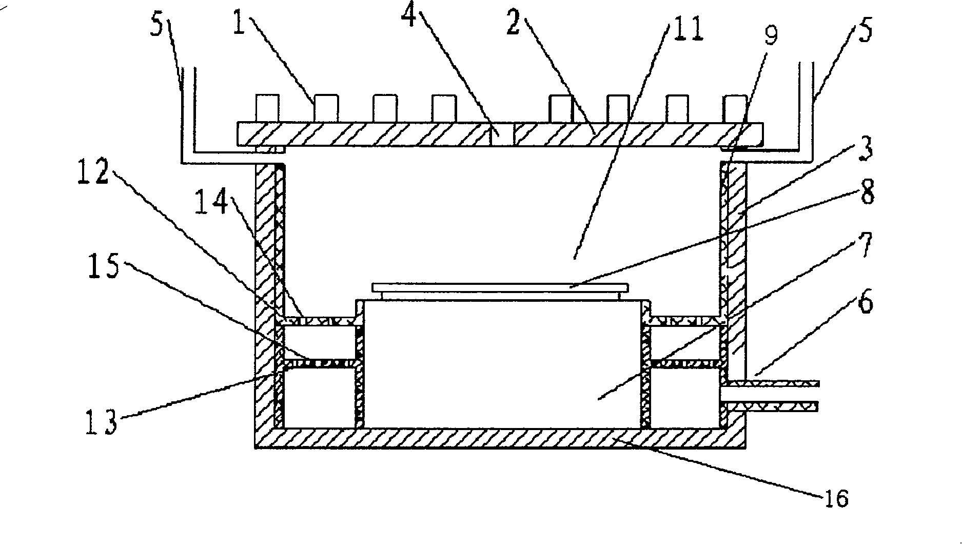
[0028] The reaction chamber lining of the present invention is mainly used to protect the wall of the reaction chamber. The reaction chamber mentioned here mainly refers to the reaction chamber of the semiconductor wafer processing equipment, and may also be other chambers.

[0029] Its preferred specific implementation is as figure 2 As shown, it includes a side lining 9 and a bottom lining, the bottom lining is higher than the lower edge of the side lining 9, and the bottom lining has two layers, including an upper lining 12 and a lower lining 13, and the upper inner lining The lining 12 has a plurality of upper layer lining holes 14; the lower layer lining 13 has a plurality of lower layer lining holes 15. The upper layer lining holes 14 and the lower layer lining holes 15 are preferably arranged alternately.

[0030] The bottom lining can also have multiple layers, but there is at least one layer. There are multiple lining holes on the bottom lining, so that the space ab...


PUM


Abstract

The invention discloses a reaction cavity lining and a reaction cavity including the lining, which comprises a side lining and a bottom lining, wherein, the bottom lining is higher than the lower edge of the side lining and at least one bottom lining is provided. A plurality of lining holes are arranged on the bottom lining. The reaction cavity including the lining is divided into an upper space and a lower space. The upper space is communicated with the lower space through the lining hole. The technics air coming from an air inlet into the reaction cavity can only be pumped from an air outlet by passing the lining hole on the bottom lining. The air flowing speed in the reaction cavity tends to be even, thus protecting the wall of the cavity and allowing uniform distribution of air in the cavity. When the wafer is performed with etching technics in the cavity, the surface of entire wafer can acquire uniform etching speed rate. The invention is mainly applicable to the reaction cavity for the semi-conductor manufacture device, also applicable to other similar cavities.

Description

technical field [0001] The invention relates to a semiconductor processing equipment component, in particular to a reaction chamber and its lining. Background technique [0002] Semiconductor wafer processing includes chemical vapor deposition (CVD) of layers of metal, dielectric, and semiconductor materials, such deposition processes including etching of these layers, polishing of photoresist mask layers, and the like. In the case of etching, plasma etching is commonly used to etch metal layers, dielectric layers and semiconductor materials. A parallel-plate plasma reactor generally includes a reaction chamber in which the silicon wafer is etched. After entering the reaction chamber, the etching gas is ionized by electrodes into plasma, and the plasma etches the wafer in the reaction chamber. [0003] During the plasma etch process, the gas is ionized to form a plasma by adding a large amount of energy to the gas at a lower pressure. By adjusting the potential of the wafe...

Claims


Application Information

Patent Timeline
Patent Type & Authority Applications(China)
IPC IPC(8): H01L21/00H01L21/3065H01L21/205H01L21/67C23C16/00C23F4/00H01J37/32H05H1/00
Inventor 管长乐
Owner BEIJING NAURA MICROELECTRONICS EQUIP CO LTD
Why Eureka
Try Eureka