Method for altering mechanical and optical performance of thin film

A technology of optical performance and mechanics, applied in the fields of electrical components, semiconductor/solid-state device manufacturing, circuits, etc., can solve the problems of high production cost, difficult to manufacture large-scale devices, complex thin film structure and manufacturing process, etc., to achieve easy control, change Physical properties, obvious effects

Inactive Publication Date: 2008-06-11
UNIV OF ELECTRONICS SCI & TECH OF CHINA
View PDF6 Cites 16 Cited by
  • Summary
  • Abstract
  • Description
  • Claims
  • Application Information

AI Technical Summary

Problems solved by technology

[0005] The Chinese patent CN 1964002A of R. Suanahayanan Yael et al. published on May 16, 2007 describes another method. This patent adds a layer in the middle of two layers of amorphous silicon nitride film The intermediate layer of different stresses is used to adjust the stress gradient of the film and prepare a stress-controlled silicon nitride film. This technical solution belongs to a new method, but its film structure and manufacturing process are complicated, the production cost is high, and it is not easy to apply in devices. in the mass production of

Method used


Image

  • Method for altering mechanical and optical performance of thin film
  • Method for altering mechanical and optical performance of thin film
  • Method for altering mechanical and optical performance of thin film

Examples


Embodiment Construction

[0024] The present invention will be further described below in conjunction with the accompanying drawings and embodiments.

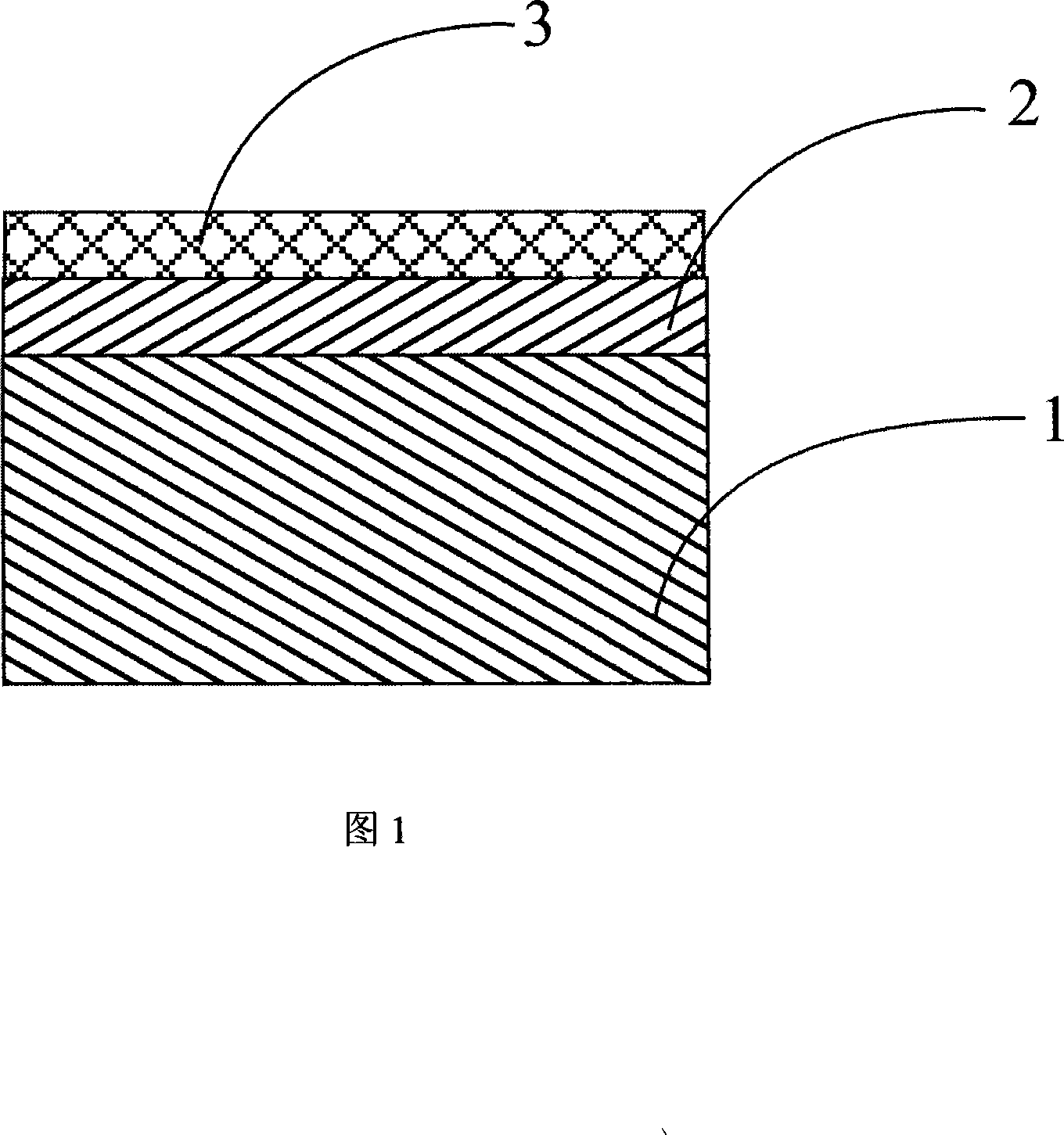
[0025] The guiding principle of the present invention is to suppress the tensile stress of the surface amorphous silicon nitride film 3 through the compressive stress of the lower amorphous silicon dioxide transition layer 2 in the composite double-layer film structure, and prepare a low-stress composite film, as shown in the figure 1. The preparation examples of the present invention are as follows: 1. select silicon wafers as the substrate 1 for thin film growth, first process with Piranha solution and clean with deionized water, then soak with dilute hydrofluoric acid solution, dry with nitrogen, and put Into the plasma enhanced (PECVD) system, vacuum; ② on the surface of the silicon substrate, with SiH 4 and N 2 O is used as the reaction gas, and a layer of amorphous silicon dioxide transition layer 2 with a thickness of 50-1500 nm is grown at 300...


PUM


Abstract

The invention discloses a method for changing the mechanics and optical performances of membrane, which is characterized in that an amorphous silicon dioxide transition layer with pressing stress is arranged on a substrate, and then an amorphous silicon nitrogen membrane with tension stress is arranged on the transition layer. The method overcomes the drawback in the prior art and improves original cragged stress grads by simple overlapping of common membrane with similar characteristic and opposite stress, thereby increasing the light reflection rate of amorphous silicon nitrogen membrane by reducing the tension stress of the membrane, and correspondingly reducing hardness and young modulus of the membrane, so that the stress of special membrane can be effectively controlled. A low stress silicon nitrogen membrane with low internal stress can be prepared, thus improving the working performance of the membrane, reducing cost of raw material and being suitable for large-scale industrialized production.

Description

technical field [0001] The invention relates to the technical field of thin films of semiconductor devices, in particular to a method for changing the mechanical and optical properties of thin films. Background technique [0002] The magnitude of film stress directly affects the morphology of materials and devices, and in severe cases, it will cause warping and cracking of the film layer, and even cause serious damage to the device. Not only that, but thin film stress can have a huge impact on the material's properties. For example, the strained silicon technology widely used in semiconductor manufacturing in recent years is to use a certain degree of biaxial or uniaxial film stress (usually diastolic pressure) to greatly increase the mobility of electrons and holes in silicon. , resulting in an increase in device operating speed and a reduction in energy consumption (see M. Leong, B. Doris, J. Kedzierski, K. Rim, M. Yang, Science, 306, 2057-2060 (2004)). Therefore, thin f...

Claims


Application Information

Patent Timeline
Patent Type & Authority Applications(China)
IPC IPC(8): H01L21/314H01L21/316H01L21/318
Inventor 许向东蒋亚东张良昌吴志明袁凯
Owner UNIV OF ELECTRONICS SCI & TECH OF CHINA
Why Eureka
Try Eureka