Method for etching suspending type etch blocking layer contact hole in embedded flash memory device

A technology for etching barrier layers and flash memory devices, which is used in semiconductor/solid-state device manufacturing, electrical components, circuits, etc., and can solve problems such as loss of metal contact silicide, so as to reduce leakage loss, cut through depth, and reduced effect

Active Publication Date: 2008-06-18
SHANGHAI HUAHONG GRACE SEMICON MFG CORP
View PDF0 Cites 13 Cited by
  • Summary
  • Abstract
  • Description
  • Claims
  • Application Information

AI Technical Summary

Problems solved by technology

[0007] The technical problem to be solved by the present invention is to provide an etching method for the contact hole of the suspended etching barrier layer in an embedded flash memory device, which solves the problem of the metal on the top of the polycrystalline gate and the active region caused by the lack of an etching barrier layer. contact silicide excess loss

Method used


Image

  • Method for etching suspending type etch blocking layer contact hole in embedded flash memory device
  • Method for etching suspending type etch blocking layer contact hole in embedded flash memory device
  • Method for etching suspending type etch blocking layer contact hole in embedded flash memory device

Examples


Embodiment Construction

[0027] Below in conjunction with accompanying drawing and embodiment the present invention will be further elaborated:

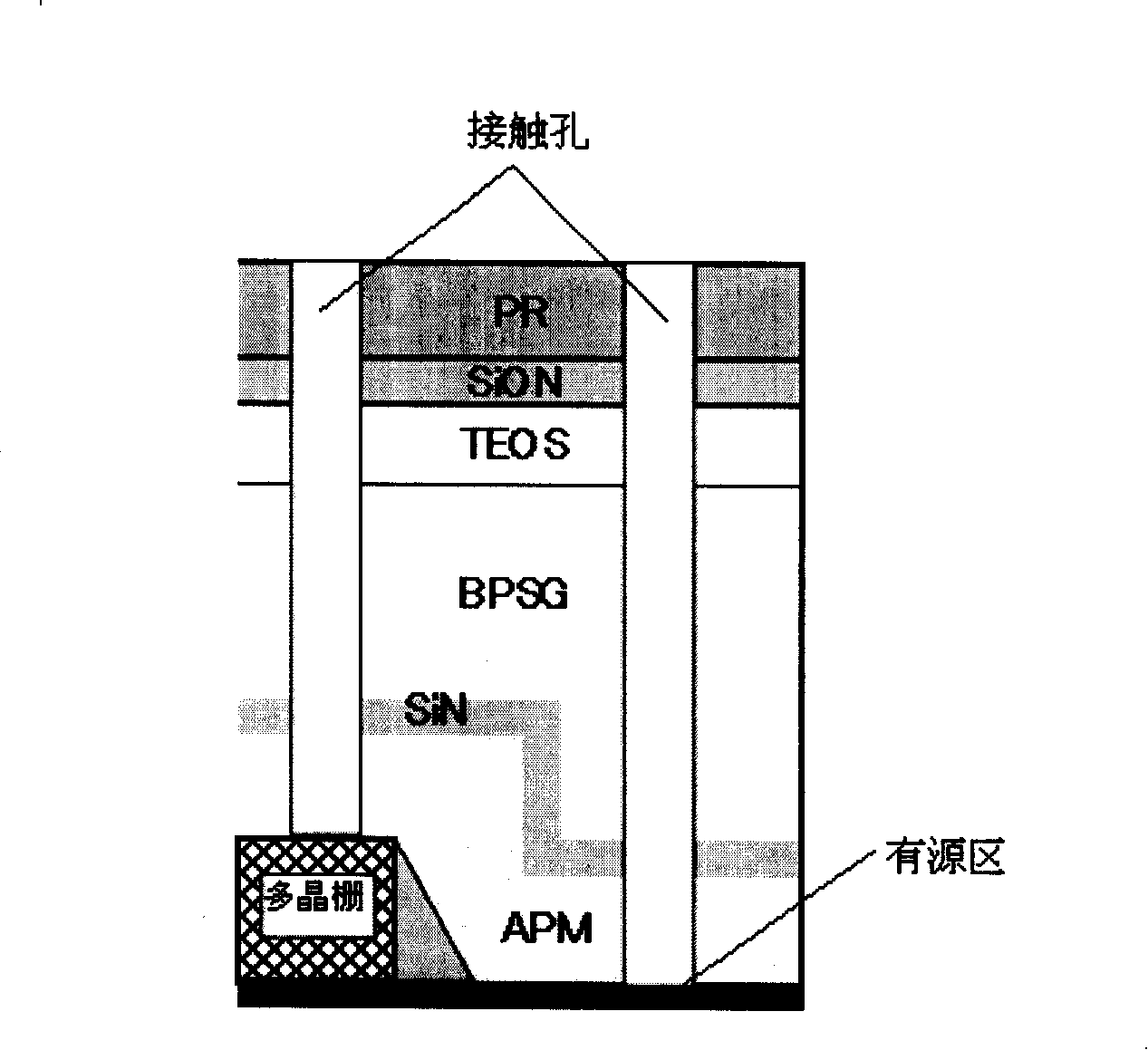
[0028] Since the etching of the contact hole needs to be etched sequentially from top to bottom DARC (SiON) / TEOS / BPSG / SiN / APM (see figure 1 ), so for films of different materials, use corresponding etching conditions.

[0029] The first step: etching of the top silicon oxynitride. If this layer of film is not etched clean (silicon oxynitride remains), it will affect the etching of the oxide film, and the opening will stop halfway (etch stop). Main parameters of this step: pressure 30-90 millitorr; upper / lower electrode power: 800-1200 / 800-1200 watts; argon 150-250sccm; trifluoromethane 15-25sccm; oxygen 5-25sccm; back helium pressure: 4-12 Torr in the middle, 10-20 Torr in the edge.

[0030] The second step: the rapid etching of the main etching of the oxide film. Considering the requirements of production efficiency, this step adopts the conditions of h...


PUM


Abstract

The invention discloses an etching method for contact holes of a suspended type etching barrier layer of an embedded flash memory device and comprises the following steps: the first step is the etching of top silicon oxy-nitride; the second step is the fast main etching of an oxide film; the third step is the slow main etching of the oxide film: in the step, the selectivity-ratio of silicon oxide to silicon nitride is bigger than 20:1, while the etching rate is relatively slower; the fourth step is to remove polymers which are produced in the previous three steps and are left at bottom parts of the contact holes; the fifth step is to remove the suspended type etching barrier layer of the nitride silicon; the sixth step is the etching of the oxide film at the bottom part. The invention solves the problem of excessive loss of metal contact silicide on the top part of a poly gate due to no etching barrier layer; at the same time, the invention can effectively avoid excessive etching and communication of the poly gate and an isolated edge of a shallow groove caused by deviation of exposing positions, thus the loss of electric leakage of the device can be reduced.

Description

technical field [0001] The invention relates to an integrated circuit semiconductor manufacturing process method, in particular to an etching method for a contact hole of a suspended etching barrier layer in an embedded flash memory device. Background technique [0002] In the manufacturing process of radio frequency devices for embedded flash memory devices, it is necessary to make contact holes (Contact) in the pre-metal dielectric (PMD) to provide electrical channels between the active region and the first metal layer. [0003] Such as figure 1 As shown, the existing contact hole manufacturing process is: after completing the metal contact (silicide) process in the active region, silicon oxide (APM), silicon nitride (SiN), boron Phosphosilicate Glass (BPSG), Atmospheric Pressure Silicon Oxide (TEOS) and Top Silicon Oxynitride (SiON, or DARC). Then apply photoresist (PR), expose the mask to make patterns, and finally perform plasma dry etching. For all device processes,...

Claims


Application Information

Patent Timeline
Patent Type & Authority Applications(China)
IPC IPC(8): H01L21/768H01L21/311
Inventor 王函吕煜坤
Owner SHANGHAI HUAHONG GRACE SEMICON MFG CORP
Why Eureka
Try Eureka