Optical beam collimation method for laminated impulse semiconductor laser
A semiconductor and laser technology, applied in the fields of optics, instruments, optical components, etc., can solve the problems that it is difficult to take into account the discreteness, collimation, and low coupling efficiency of stacked pulsed semiconductor lasers.
- Summary
- Abstract
- Description
- Claims
- Application Information
AI Technical Summary
Problems solved by technology
Method used
Image
Examples
Embodiment Construction
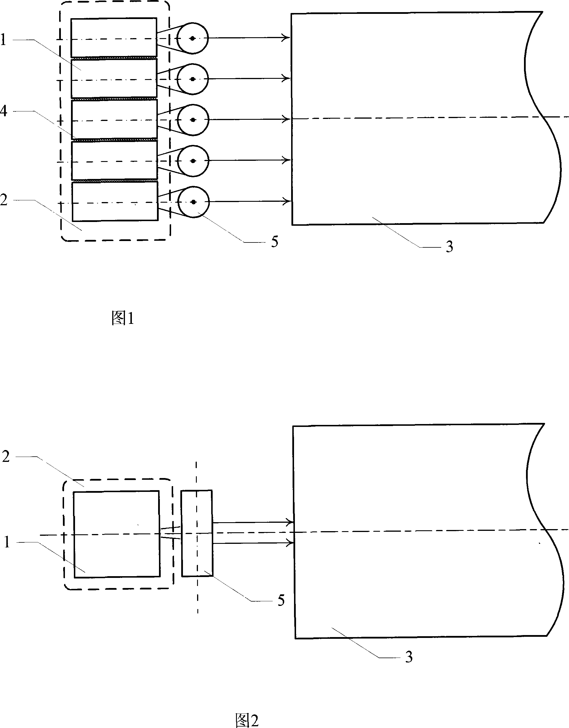
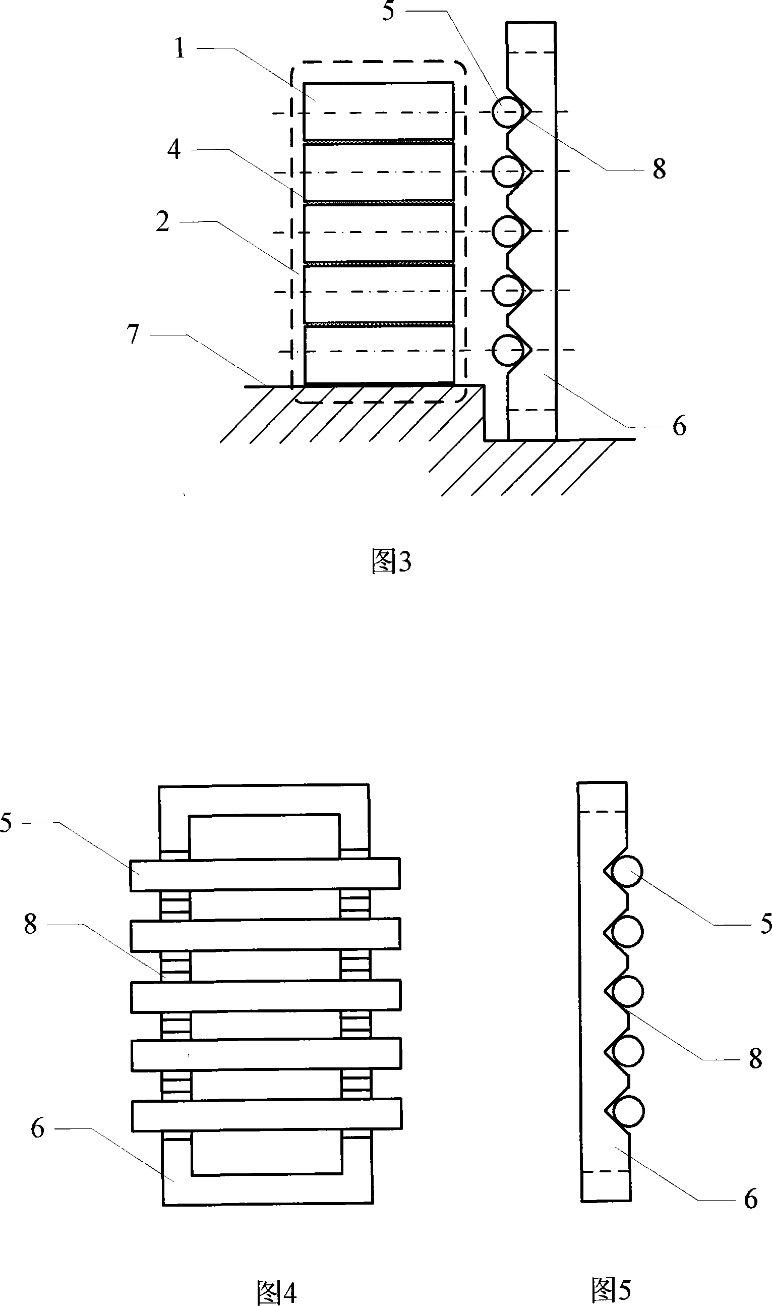
[0007] The present invention is realized in this way, as shown in FIG. 3 , a collimating lens holder 6 is used, which is vertically erected on the heat sink 7 . The collimating lens holder 6 is a rectangular frame, which is made by etching a rectangular portion in the middle of a rectangular GaAs sheet by photolithography. Several groups of V-shaped grooves 8 are equidistantly engraved on one side of the two long sides of the rectangle, which are respectively opposite to several single tubes 1 in the stacked pulsed semiconductor laser 2 for placing the collimating cylindrical lens 5 . Five single tubes 1 are used, the thickness of each single tube 1 is 100±10 μm, and the thickness of the welding layer 4 between adjacent single tubes 1 is 15±5 μm. The light emitting area of each single tube 1 is opposite to a V-shaped groove 8 on the collimating lens holder 6 . An existing five-dimensional precision adjusting frame is used to clamp the collimating lens holder 6, and its post...
PUM
 Abstract
Description
Claims
Application Information

