Dynamic bandwidth compensating method and associated apparatus

A technology for programming gain and amplifiers, applied to parts of amplifying devices, parts of controlling amplifying devices, amplifiers, etc.

Active Publication Date: 2008-07-16
MEDIATEK INC
View PDF0 Cites 14 Cited by
  • Summary
  • Abstract
  • Description
  • Claims
  • Application Information

AI Technical Summary

Problems solved by technology

[0009] However, the programmable gain amplifier used in the digital video tuner system must provide the same bandwidth for different gain values

Method used


Image

  • Dynamic bandwidth compensating method and associated apparatus
  • Dynamic bandwidth compensating method and associated apparatus
  • Dynamic bandwidth compensating method and associated apparatus

Examples


Embodiment Construction

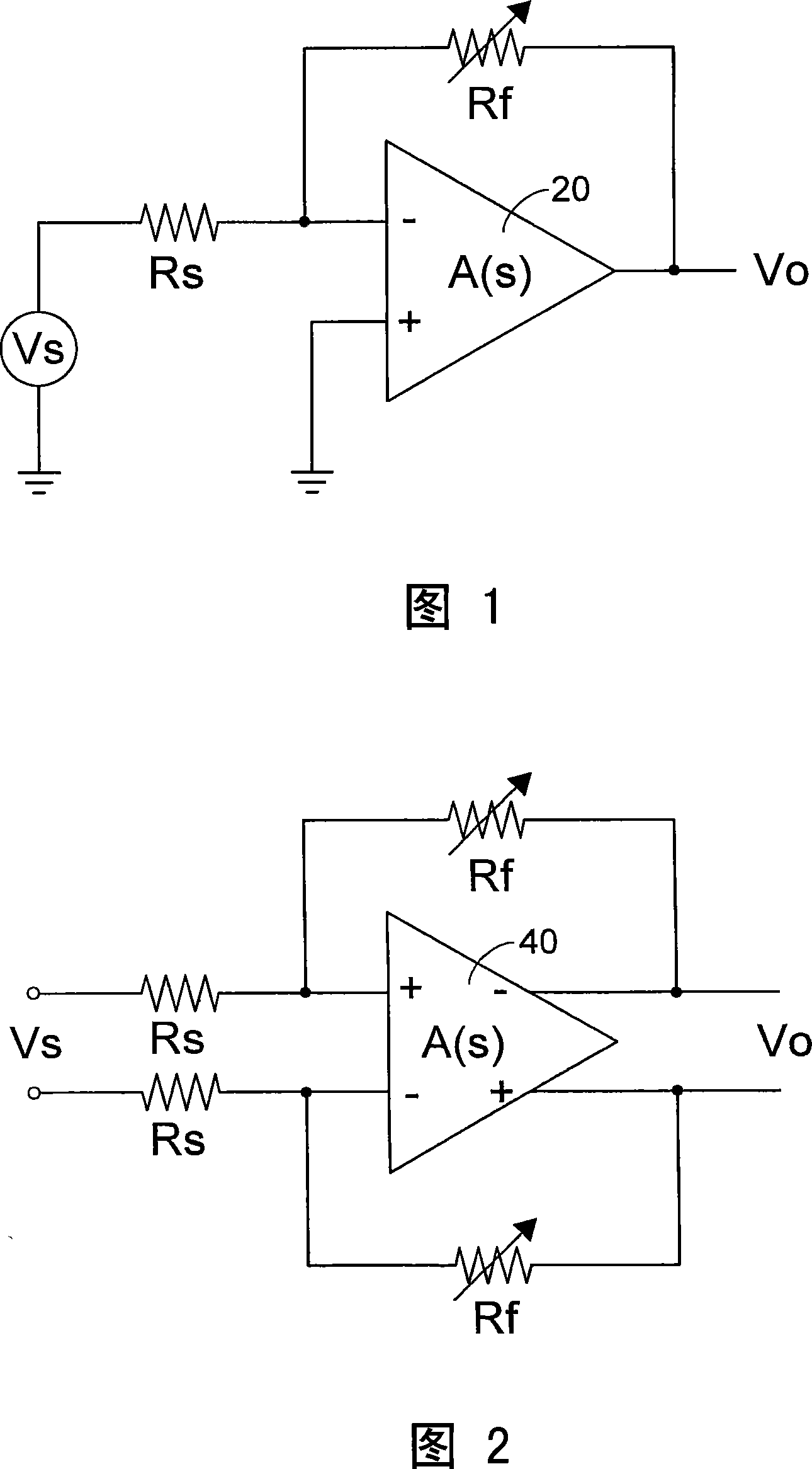
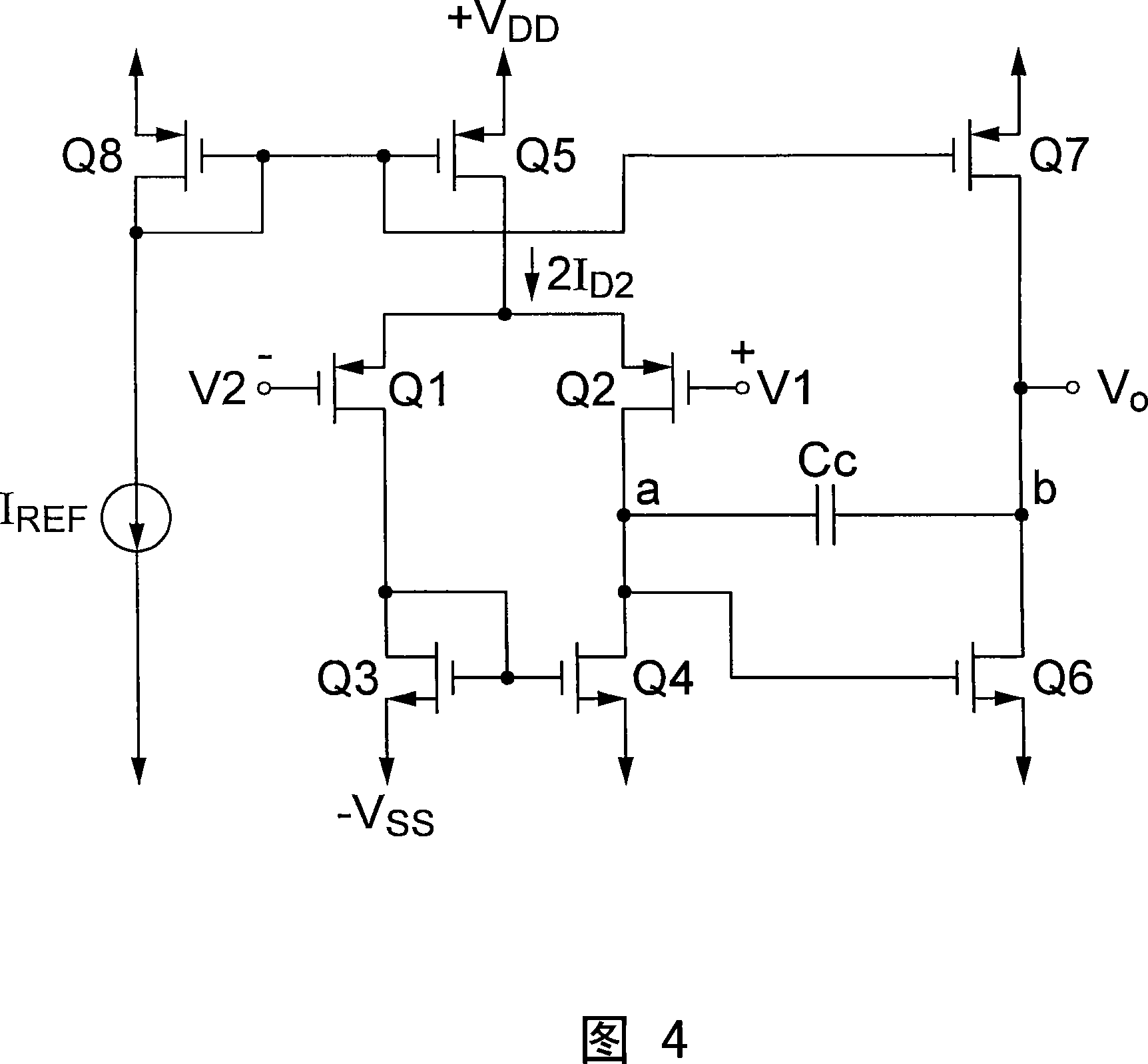
[0054] Please refer to FIG. 4 , which is a circuit diagram of a two-stage complementary metal-oxide semiconductor (CMOS) operational amplifier. The current mirror formed by the transistors Q8 and Q5 provides the bias current of the first-stage amplifying circuit; the current mirror formed by the transistors Q8 and Q7 provides the bias current of the second-stage amplifying circuit. The first-stage amplifying circuit is composed of a differential pair of transistors Q1 and Q2 and active loads of transistors Q3 and Q4, and the transistors Q3 and Q4 form a current mirror. The second-stage amplifying circuit includes a common-source amplifier of transistor Q6 and a dynamic load of transistor Q7. The output end (node ​​a) of the first-stage amplifying circuit is connected to the input end (gate of transistor Q6 ) of the second-stage amplifying circuit. Therefore, the transistors Q1 and Q2 are the two input terminals of the operational amplifier, and the drain (node ​​b) of the tra...


PUM


Abstract

The invention relates to a dynamic compensation method and a related device of a programmable gain amplifier. The programmable gain amplifier includes: an operational amplifier connected to a plurality of resistors, so that the operational amplifier can realize closed feedback control and has a closed-loop gain as the right formula; wherein, β is a feedback factor, which can be determined by the plurality of resistors The resistance value is determined, and A(s) is the open-loop gain of the operational amplifier, and the operational amplifier includes a first-stage amplifying circuit and a second-stage amplifying circuit, and a variable compensation capacitor is provided in the first-stage amplifying circuit Between the output end of the second-stage amplifying circuit and the output end of the second-stage amplifying circuit, the main pole of the open-loop gain of the operational amplifier can be changed as the capacitance value of the variable compensation capacitor changes. The invention can adjust the bandwidth of the operational amplifier by changing the equivalent capacitance value of the variable compensation capacitor.

Description

technical field [0001] The present invention relates to a dynamic compensation method and a related device of a programmable gain amplifier (programmable gain amplifier, PGA), and in particular to a dynamic compensation method and a related device that utilizes an internal variable compensation capacitor to have the same bandwidth at different gains. device. Background technique [0002] Please refer to FIG. 1 , which is a schematic diagram of a conventional programmable gain amplifier. Generally, the programmable gain amplifier includes an operational amplifier (operational amplifier, referred to as OP) 20 , a feedback resistor (Rf), and a resistor (Rs). The input signal (Vs) is input to the negative input terminal of the operational amplifier 20 through the resistance (Rs), the positive input terminal of the operational amplifier 20 is connected to the ground terminal, and the output terminal (Vo) of the operational amplifier 20 is connected to the negative input terminal...

Claims


Application Information

Patent Timeline
IPC IPC(8): H03F3/45H03G1/00
CPCH03F1/083H03F3/45085H03F3/45183H03F3/45475H03F2200/153H03F2203/45512H03F2203/45514H03F2203/45522H03G5/24H03H11/126H03H11/1291
Inventor 林珩之
Owner MEDIATEK INC
Why Eureka
Try Eureka