Blind hole plate and its processing method

A processing method and blind hole board technology, which are applied in the formation of electrical connection of printed components, manufacturing of multi-layer circuits, and electrical connection of printed components, etc., can solve the problems of lowering product qualification rate and large cost impact, and achieve the reduction of processing costs and the reduction of working procedures. The effect of reducing and preventing accidents

Inactive Publication Date: 2008-07-16
DALIAN PACIFIC ELECTRONICS
View PDF0 Cites 23 Cited by
  • Summary
  • Abstract
  • Description
  • Claims
  • Application Information

AI Technical Summary

Problems solved by technology

Although the circuit board processed by the above method has a flat surface at the position of the blind hole and no bulge on the surface after being subjected to thermal shock, it also has certain deficiencies. One process increases the processing cycle and processing cost to varying degrees, and the increase in the process also reduces the pass rate of the product, which has a greater impact on the cost of the entire product

Method used


Image

  • Blind hole plate and its processing method
  • Blind hole plate and its processing method
  • Blind hole plate and its processing method

Examples


Embodiment Construction

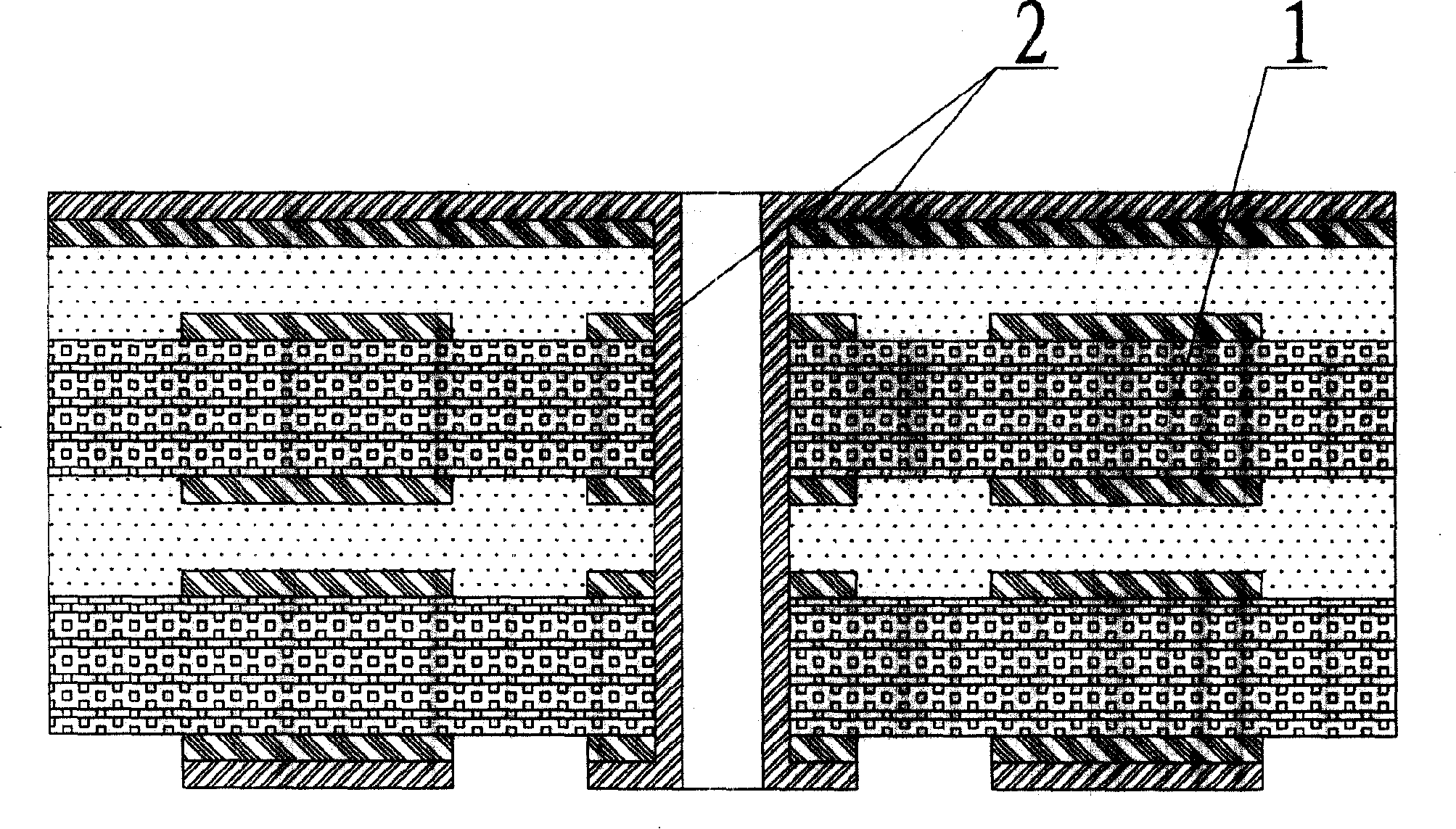
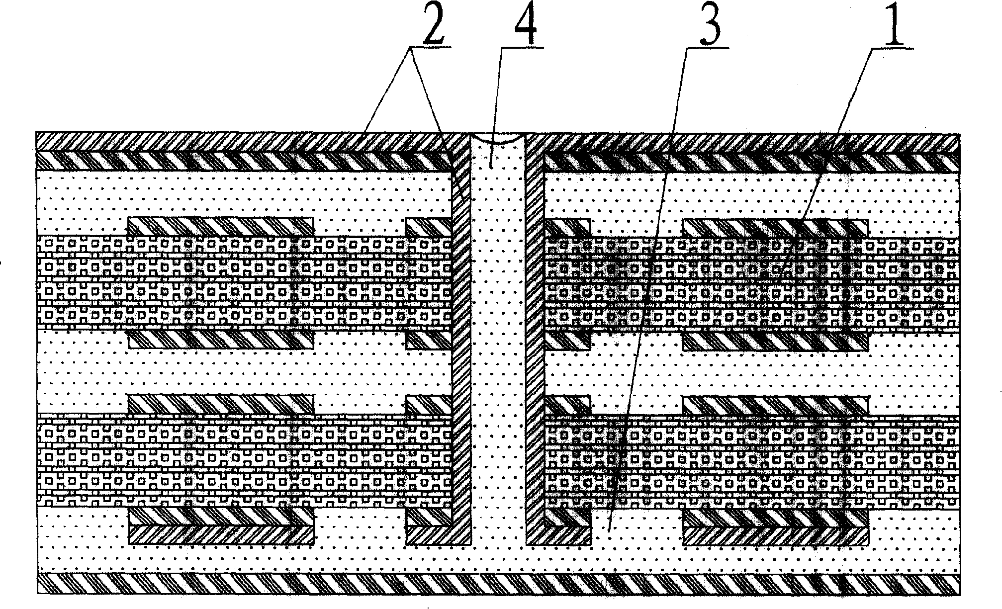
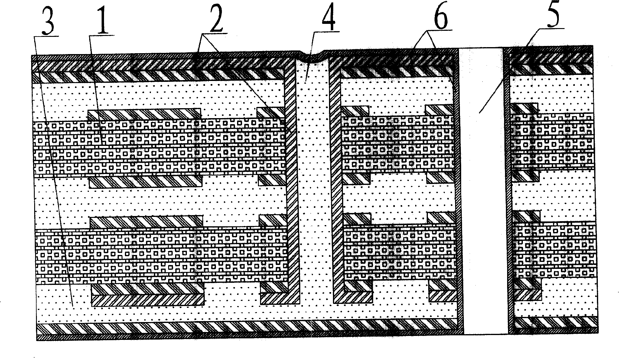
[0030] First, laminate the multi-layer board 1 corresponding to the number of layers of blind holes, then drill holes on the multi-layer board, and plate copper 2 on the hole wall, as in figure 1 shown. The above-mentioned multi-layer board is used as a sub-board and another layer of sub-board 3 is laminated twice, and the resin in the prepreg fills the hole after copper plating to form a blind hole 4, such as figure 2 shown. Drill through holes 5 and electroless copper plating on multilayer boards containing blind holes, so that a layer of copper 6 is attached to both sides of the drilled through holes and the circuit board, such as image 3 shown. Make a film for graphic transfer, make the part corresponding to the blind hole on the graphic film into a light-transmitting area smaller than the diameter of the blind hole, and paste a photosensitive dry film 7 on the surface of the blind hole multilayer board, which will be used for graphic transfer The film 8 is pasted on ...


PUM


Abstract

The invention provides a blind orifice plate, wherein a welding disk on the top of a blind hole is provided with a through hole for relieving stress. The main method for processing the blind orifice plate is that: on the basis of the prior technology, only a part on a graphics film corresponding to the blind hole is made into a phonic zone which is smaller than the blind hole in diameter during the course of making graphics film. In the invention, the working procedure of 'processing-jacking hole with resin -curing-lapping' is deleted, the manufacturing circle is shortened and the processing cost is decreased correspondingly because the working procedure is reduced; after the process is reduced, the overall qualified product rate is improved. The invention is a modification on related design during the pre-production of film, which does not change the prior production technology; the operator can conduct normal operation according to the prior procedures, which avoids unnecessary accidents. The product of the invention can meet the requirements of consumers in terms of overall appearance and performance and the user is not affected to use the product.

Description

technical field [0001] The invention relates to a processing method of a circuit board. Background technique [0002] With the continuous development of science and technology, the types of circuit boards closely related to it are also increasing. Circuit boards with blind holes (abbreviated as blind hole boards) are a more popular type in recent years. The processing of this kind of circuit board can continue to use the traditional process method, the main content of which is to process the multilayer board corresponding to the part containing the blind hole, drill the multilayer board, and carry out copper plating on the hole, and then place the part containing the blind hole. The holed multilayer board is laminated together as a sub-board (X layer) with another sub-board (Y layer), and the resin contained in the prepreg fills the holes in the holed sub-board (X layer) between the two, Blind holes are formed, and then through-holes (X+Y layers) are drilled on the laminat...

Claims


Application Information

Patent Timeline
Patent Type & Authority Applications(China)
IPC IPC(8): H05K1/11H05K3/46H05K3/42
Inventor 孙其方李勇张伟王大伟
Owner DALIAN PACIFIC ELECTRONICS
Why Eureka
Try Eureka