Method for realizing portion exhaust insulators upper silicon device physical contact

A technology of silicon-on-insulator and body contact, which is applied in semiconductor/solid-state device manufacturing, electrical components, circuits, etc., can solve the problems that the floating body effect cannot be completely suppressed, the floating body effect cannot be effectively suppressed, and the leakage current is too large, so as to achieve the purpose of suppressing the floating body Effect, low cost, simple process

Inactive Publication Date: 2008-07-30
INST OF MICROELECTRONICS CHINESE ACAD OF SCI
View PDF0 Cites 7 Cited by
  • Summary
  • Abstract
  • Description
  • Claims
  • Application Information

AI Technical Summary

Problems solved by technology

But this method cannot effectively suppress the floating body effect, and causes excessive leakage current
[0009] Literature "Liu Yunlong, Liu Xinyu, et.al, "Simulation of a Novel Schottky Body-Contacted Structure Suppressing Floating Body Effect in Partially-Depleted SOI nMOSFET's", CHINESE JOURNAL OFSEMICONDUCTOR, Vol.23, No.10, p.1019, Oct.2002" proposed the Schottky contact technology, using the thick silicide in the source region to form a Schottky contact with the body region under the source region to clamp the body potential, but this method still has the problem of body resistance, and due to the Schottky barrier Exist, can not completely suppress the floating body effect

Method used


Image

  • Method for realizing portion exhaust insulators upper silicon device physical contact
  • Method for realizing portion exhaust insulators upper silicon device physical contact
  • Method for realizing portion exhaust insulators upper silicon device physical contact

Examples


Embodiment

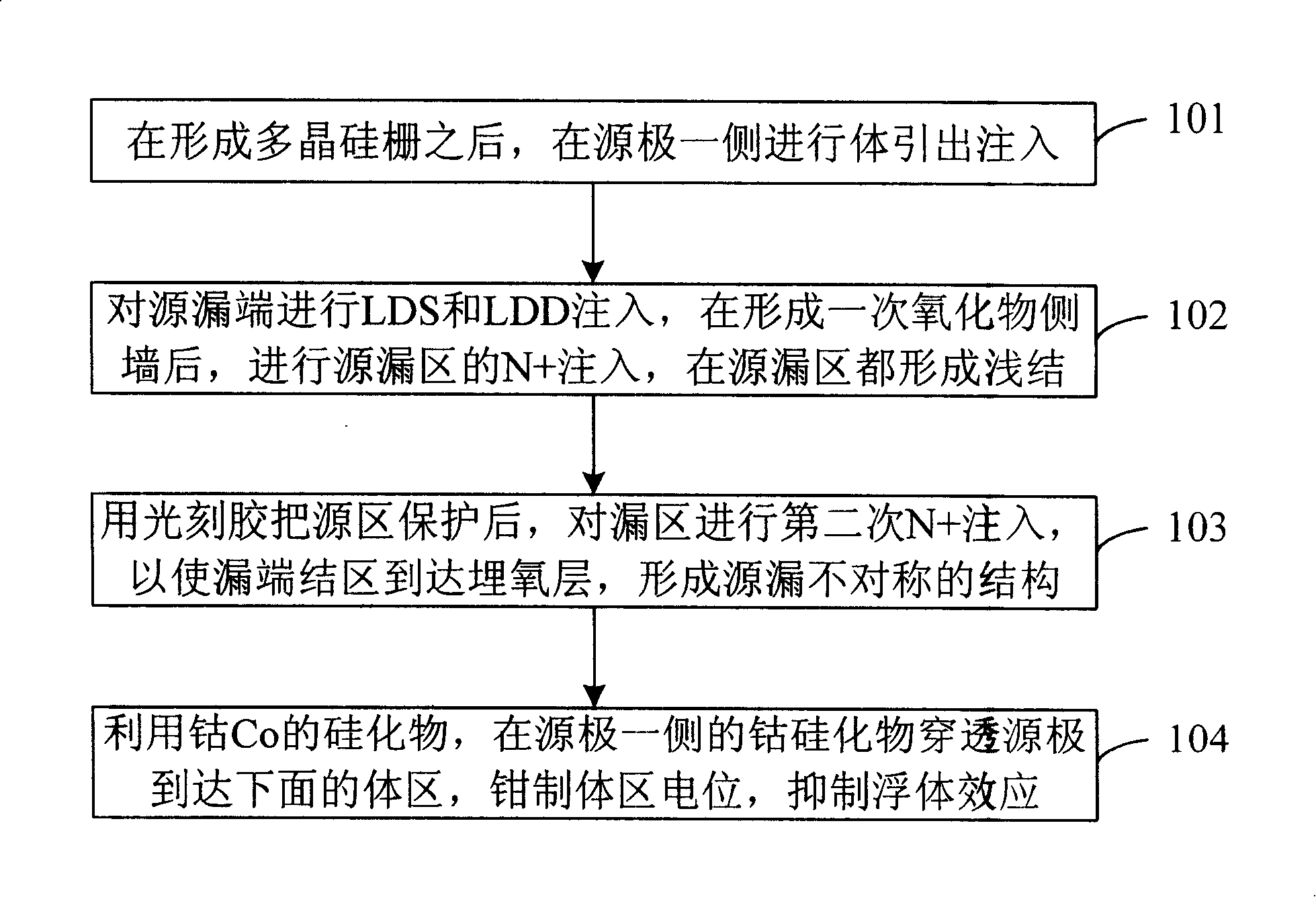
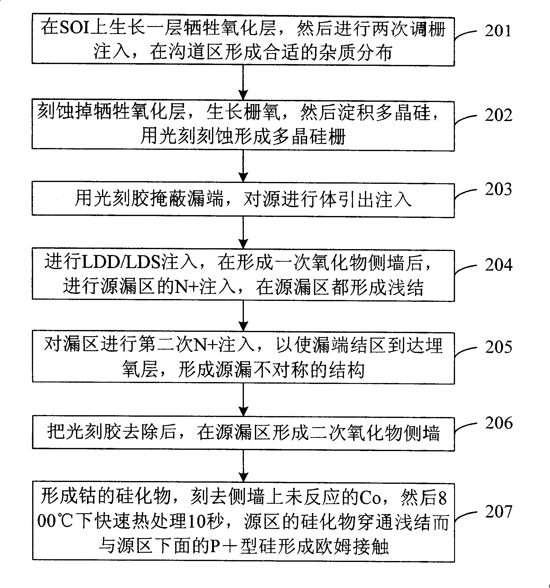
[0046] Such as figure 2 as shown, figure 2 A flowchart of a method for realizing body contact of a partially depleted SOI device according to an embodiment of the present invention, the method includes the following steps:

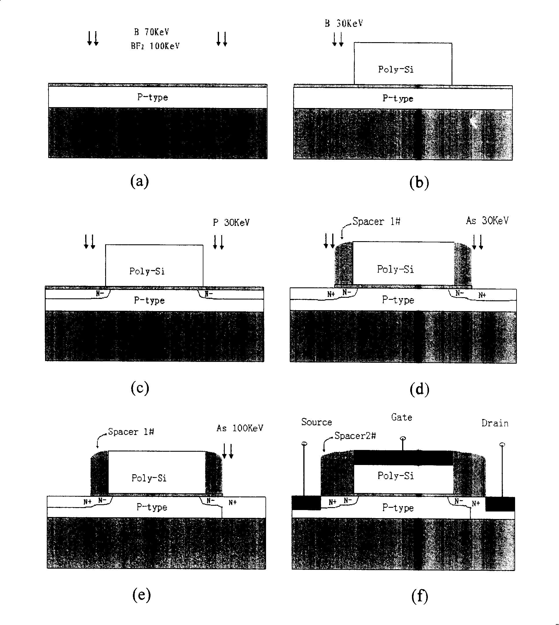
[0047] Step 201: first grow a sacrificial oxide layer on the SOI, and then perform gate adjustment implantation twice to form a proper impurity distribution in the channel region. Such as image 3 Shown in (a).

[0048] Step 202: Etching away the sacrificial oxide layer, growing gate oxide, then depositing polysilicon, and forming a polysilicon gate by photolithography. Such as image 3 Shown in (b).

[0049]Step 203: Mask the drain end with photoresist, and perform body extraction implantation on the source; for example image 3 Shown in (b).

[0050] In this step, high-dose and high-energy boron ion implantation is performed for SOI NMOSFET to form a high-concentration P+ region under the source. For SOI PMOSFETs, high-dose and high-energy phos...


PUM


Abstract

The invention relates to the technical field of body contact of SOI devices in the semiconductor technology, and discloses a method for achieving body contact of some depleted SOI devices. The invention comprises the following steps: A. after a polysilicon gate is formed, a body is led out and injected on one side of a source electrode; B. LDS and LDD are injected into source/drain ends; after a primary oxide side wall is formed, N+ is injected into source/drain areas to form shallow junctions in the source/drain areas; C. after the source area is protected with photosensitive resist, the drain area is injected with N+ for the second time so that a junction area on the drain end reaches a buried oxide layer, thus forming a source/drain unsymmetrical structure; D. cobaltic silicide is used; the cobaltic silicide on one side of a source electrode penetrates the source electrode and reaches a body area below, which limits the potential of the body area and inhibits floating effect. By adopting the invention, not only the floating effect is effectively inhibited, but also the performance of some depleted SOI devices is improved. In addition, the invention is compatible with standard complementary metal-oxide-semiconductor transistors, and has the advantages of simple process, low cost and so on.

Description

technical field [0001] The invention relates to the technical field of silicon-on-insulator (SOI) device body contact in semiconductor technology, in particular to a method for realizing the body contact of a partially depleted silicon-on-insulator device. Background technique [0002] As device feature sizes shrink, Moore's Law is being tested more and more severely. Whether Moore's Law can continue to develop depends on the emergence of innovative technologies. In recent years, many innovative technologies have emerged, such as FinFET, single-electron devices, and double-gate devices, among which SOI technology has the greatest development potential. [0003] There are two types of SOI devices: partially depleted and fully depleted. Fully depleted device Because the silicon film is completely depleted when the device is working, the potential barrier between the source and the body is very small, so the holes accumulated in the body region can flow out through the source...

Claims


Application Information

Patent Timeline
Patent Type & Authority Applications(China)
IPC IPC(8): H01L21/336H01L21/84
Inventor 王立新
Owner INST OF MICROELECTRONICS CHINESE ACAD OF SCI
Why Eureka
Try Eureka