Semiconductor bipolar light emitting and laser devices and methods

A technology of semiconductors and laser pulses, applied in the direction of lasers, laser components, phonon exciters, etc.

Inactive Publication Date: 2008-08-06
THE BOARD OF TRUSTEES OF THE UNIV OF ILLINOIS
View PDF4 Cites 18 Cited by
  • Summary
  • Abstract
  • Description
  • Claims
  • Application Information

AI Technical Summary

Problems solved by technology

In several respects, p-type materials are considered to be more difficult to use with n-type materials, and tend to be

Method used


Image

  • Semiconductor bipolar light emitting and laser devices and methods
  • Semiconductor bipolar light emitting and laser devices and methods
  • Semiconductor bipolar light emitting and laser devices and methods

Examples


Embodiment Construction

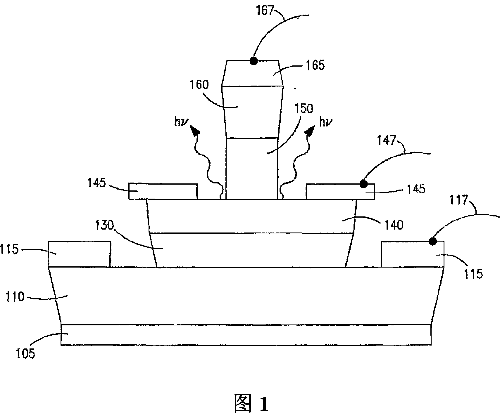
[0060] Figure 1 illustrates the device set forth in the mentioned PCT publication WO 2005 / 020287. The substrate 105 has the following layers disposed thereon: a sub-collector 110, a collector, a base 140, an emitter 150, and a cap layer 160. The collector metal (or electrode) 115, the base metal 145, and the emitter metal 165 are also shown. The collector lead 117, the base lead 147, and the emitter lead 167 are also shown. As disclosed in the mentioned co-pending application, the collector layer 130 includes 3000 angstroms thick n-type GaAs, n=2×10 16 cm -3 , The base layer 140 includes 600 angstroms thick p+ carbon doped InGaAs (1.4% In) graded in composition, p=4.5×10 19 cm -3 , The emitter layer 150 includes 800 angstroms thick n-type InGaP, n=5×10 17 cm -3 , And the cap layer includes 1000 angstroms thick n+InGaAs, n=3×10 19 cm -3 .

[0061] As disclosed in the mentioned PCT publication WO 2005 / 020287, for the traditional PN junction diode operation, the recombination process...


PUM


Abstract

The invention relates to a method for generating an optical output, said method comprising the steps of: providing first and second electrical signals; providing a bipolar light emitting transistor device comprising a collector region, a base region and an emitter region; providing a collector electrode coupled to the collector region and an emitter electrode coupled to the emitter region, and potential coupled with respect to the collector electrode and the emitter electrode; providing an optical coupling in optical communication with the base region ; providing first and second base electrodes coupled to the base region; and coupling the first and second electrical signals to the first and second base electrodes, respectively, to generate The region emits and couples into the optical coupling an optical output that is a function of the first and second electrical signals. The present invention also discloses an improved pnp transistor laser and a technique for switching back and forth between a stimulated emission mode and a spontaneous emission mode for generating output laser pulses.

Description

Technical field [0001] The present invention relates to semiconductor light emitting and laser devices and methods, and also relates to laser transistors and techniques for enhancing high-speed optical signal generation, and also relates to devices and methods including hybrid modulation laser transistors and techniques, and also relates to PNP bipolar transistors , PNP bipolar light-emitting transistor and PNP bipolar transistor layer. Background technique [0002] Part of this background technology depends on the development of light emitters based on direct band gap semiconductors, such as III-V semiconductors. Such devices including light-emitting diodes and laser diodes are commonly used in the commercial field. [0003] Another part of this background art depends on the development of wide band gap semiconductors to obtain high minority carrier injection efficiency in devices called heterojunction bipolar transistors (HBT). It was first proposed in 1948 (see, for example, U...

Claims


Application Information

Patent Timeline
IPC IPC(8): H01S3/13
Inventor 米尔顿·冯尼克·小霍伦亚克理查德·禅加布里埃尔·沃尔特
Owner THE BOARD OF TRUSTEES OF THE UNIV OF ILLINOIS
Why Eureka
Try Eureka