
Resputtered copper seed layer

A copper target and copper metal technology, which is applied in the field of sputtering deposition, can solve the problems that copper seed crystal sputtering deposition is difficult to achieve, and the sputtering deposition of copper seed crystal layer cannot be completely coated.

Inactive Publication Date: 2008-08-13
APPLIED MATERIALS INC
View PDF2 Cites 10 Cited by
  • Summary
  • Abstract
  • Description
  • Claims
  • Application Information

AI Technical Summary

Problems solved by technology

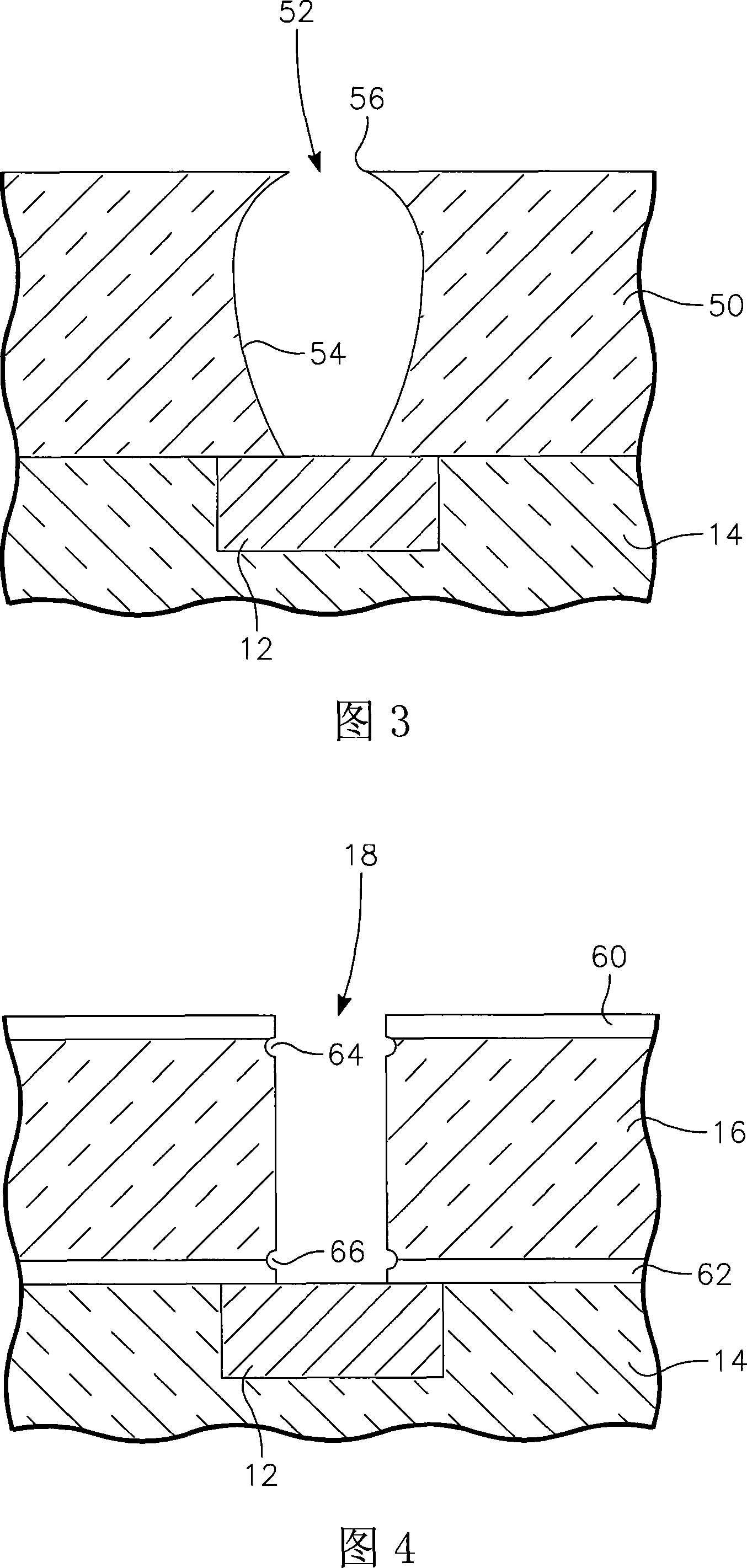
Conventional copper seed sputter deposition is difficult to reach those concave grooves 64 and 66
[0012] The sputter deposition of the copper seed layer does not completely coat the sidewalls 54 of the recess or the sides of the grooves 64, 66, causing the same problems as described above with respect to the protrusions

Method used


Image

  • Resputtered copper seed layer
  • Resputtered copper seed layer
  • Resputtered copper seed layer

Examples


Embodiment Construction

[0032] Copper filling of high aspect ratio holes, such as vias and dual damascene interconnects, is achieved by a combination of copper sputter deposition and argon or copper sputter etching, preferably performed in a single copper sputter chamber. High energy sputter etching reduces the size of the protrusions and also tends to redistribute the copper to the recessed portions of the sidewalls in a process called re-sputtering.

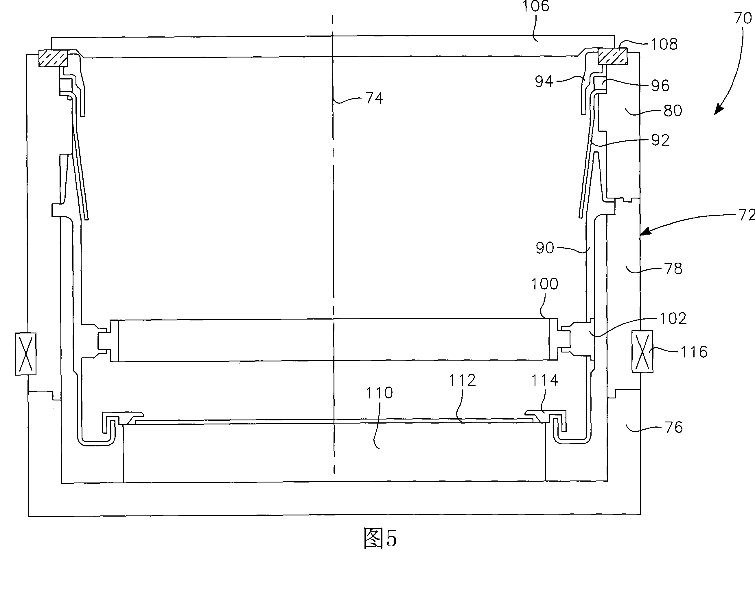
[0033] Although some aspects of the present invention are not limited thereto, sputter deposition and sputter etching are preferably performed in a chamber with RF coils that have limited excitation if there is sputtering of the copper target during the etching process. Argon plasma for argon sputter etching. Sputter Deposition / Etch Sequence for Tantalum Barriers in Inductively Coupled Sputtering Chambers in U.S. Patent Application 10 / 915,139 filed August 9, 2004 by Ding et al., now published as U.S. Patent Application Publication 2006 / 0030151 descri...


PUM

PropertyMeasurementUnit
critical dimensionaaaaaaaaaa

Abstract

The present invention discloses a comprehensive copper deposition process, particularly suitable for forming a copper seed layer in narrow through-hole features prior to electrochemical copper plating, which process includes copper sputter deposition (160) followed by At least one cycle of the step of sputter etching (162) of the deposited copper is preferably performed in the same sputter chamber. This deposition is performed under conditions that promote a high copper ionization fraction and a strong wafer bias, thereby drawing copper ions into the through-hole features. The etching can be done using argon ions, preferably inductively excited by RF coils around the chamber, or by copper ions formed at high target power and strong magnetrons or by using RF coils. Two or more deposition / etch cycles can be performed. The final flash deposition (168) can be performed under conditions of high copper ionization and low wafer bias.

Description

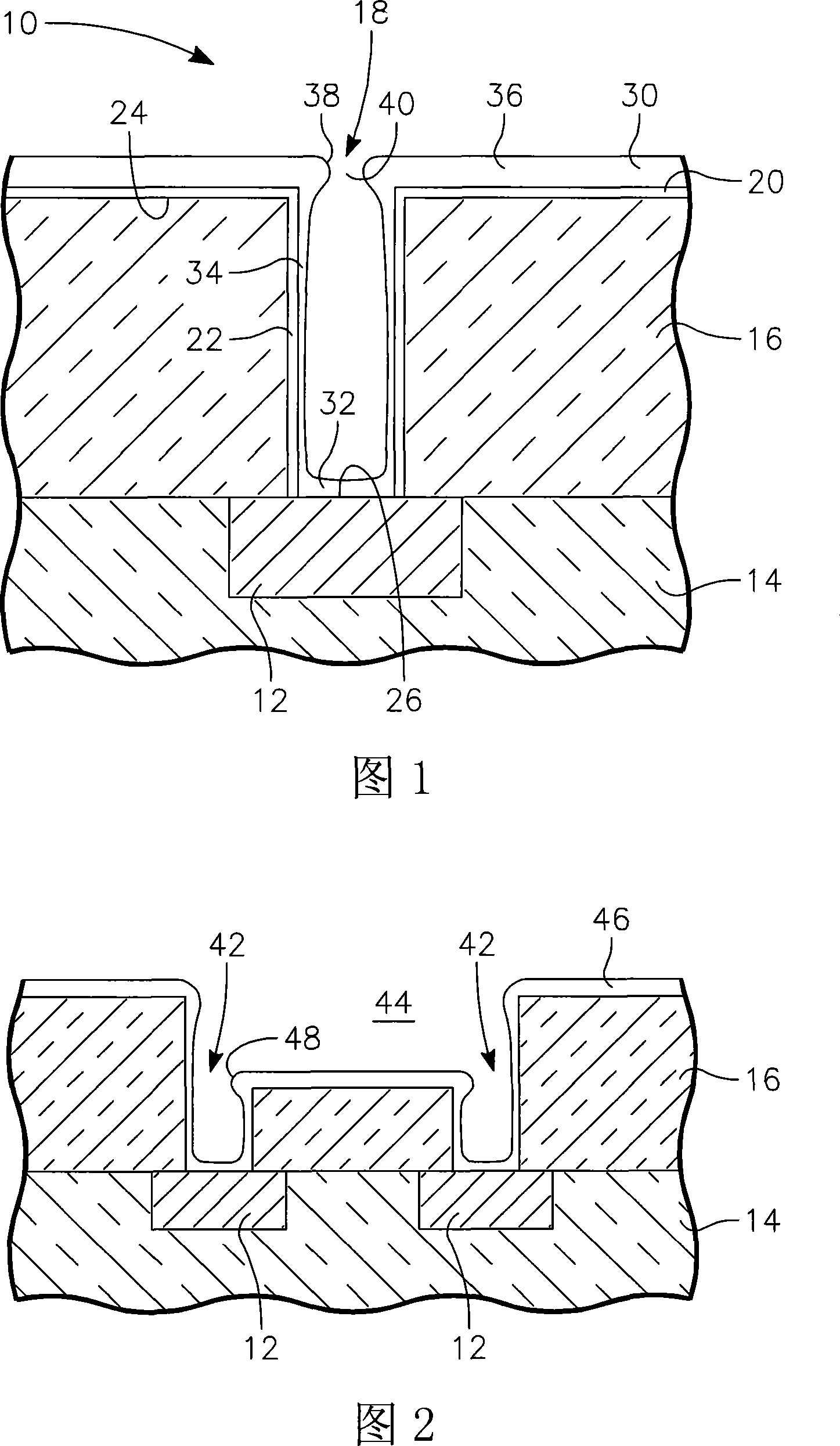
technical field [0001] The present invention relates generally to sputter deposition in the formation of semiconductor integrated circuits. More specifically, the present invention relates to the combination of sputter deposition and sputter etching in forming a liner layer. Background technique [0002] Magnetron sputtering has long been used in the deposition of horizontally extended layers of metallizations such as aluminum and copper. More recently, magnetron sputtering has been adapted for the more challenging task of depositing liner layers in high aspect ratio holes such as interlayer electrical contacts, ie vias. Via features 10 for copper metallization shown in the cross-sectional view of FIG. 1 are formed over conductive features 12 on the surface of a lower dielectric layer 14 . An upper dielectric layer 16 is deposited over the lower dielectric layer 14 and its conductive features 12 , and vias 18 are etched through the upper dielectric layer 16 to the conducti...

Claims


Application Information

Patent Timeline
Patent Type & Authority Applications(China)
IPC IPC(8): C23C14/35C23C14/14
CPCC23C14/046C23C14/165C23C14/358C23C14/5826C23C14/584H01J37/3408H01J37/3455H01L21/2855H01L21/76865H01L21/76873H01L21/76877C23C14/35C23C14/22C23C14/14
Inventor 唐先民阿维德·苏尼达瑞杰恩丹尼尔·柳伯恩罗千龚则敬阿纳塔·苏比玛尼仲华傅新宇王荣钧炯·曹吉克·于约翰·福斯特帕布拉姆·古帕拉加
Owner APPLIED MATERIALS INC
Learn More