Method for preparing p-type ZnO film by doping Sb

A thin film, p-type technology, applied in gaseous chemical plating, metal material coating process, coating, etc., can solve the problem of low doping efficiency of p-type ZnO, and achieve the effect of overcoming the difficulty of preparation

Inactive Publication Date: 2008-09-03
DALIAN UNIV OF TECH
View PDF2 Cites 18 Cited by
  • Summary
  • Abstract
  • Description
  • Claims
  • Application Information

AI Technical Summary

Problems solved by technology

[0005] The purpose of the present invention is to overcome the shortcoming of low p-type ZnO doping efficiency a...

Method used


Image

  • Method for preparing p-type ZnO film by doping Sb
  • Method for preparing p-type ZnO film by doping Sb

Examples


Embodiment 1

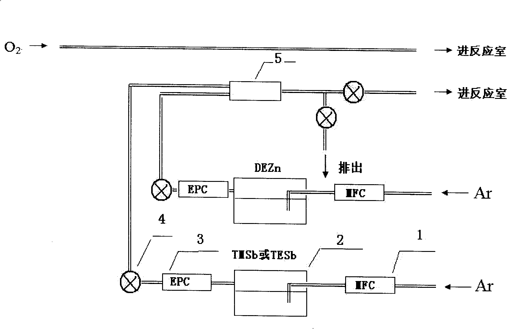
[0022] (1) Substrate cleaning treatment. Sapphire, Si, GaAs, InP, CaF for substrate 2 , quartz, and glass can be used, and the substrate can be treated with the standard cleaning process of general semiconductors.

[0023] (2) Send the cleaned substrate to the pretreatment chamber, and close the door of the sample pretreatment chamber. Start the mechanical pump to evacuate the sample pretreatment chamber until the vacuum degree of the sample pretreatment chamber reaches 50-10 -1 When Pa, turn on the mechanical pump of the reaction chamber to evacuate. When the vacuum degree of the reaction chamber and the vacuum degree of the sample pretreatment chamber are basically balanced, open the connecting gate valve to transfer the substrate to the substrate tray of the reaction chamber, and close the gate. plate valve.

[0024] (3) When the vacuum degree of the reaction chamber reaches below 10Pa, the turbomolecular pump in the reaction chamber can be started. The vacuum degree of...

Embodiment 2

[0030] This process method is substantially the same as the steps of Example 1, except that step-by-step annealing is carried out during the growth process to form a buffer layer and improve the growth quality of subsequent thin films. The specific method is to grow for a period of time (1 to 20 minutes) at 150°C to 500°C in a lower growth temperature range, then turn off the zinc source, and heat the substrate in situ to 700 to 800°C for thermal annealing. The processing time is After 1 to 30 minutes, the temperature of the substrate sheet drops to the growth temperature and then continues to grow until the required thickness is reached.

Embodiment 3

[0032] This process method is the same as the steps in Example 1, the difference is that after the growth is completed, the zinc source is turned off, and the substrate temperature is raised to 700-800°C and then annealed in oxygen to further increase the doping of p-type ZnO Quality; it can also be used simultaneously with the method of introducing a buffer layer in Example 2.
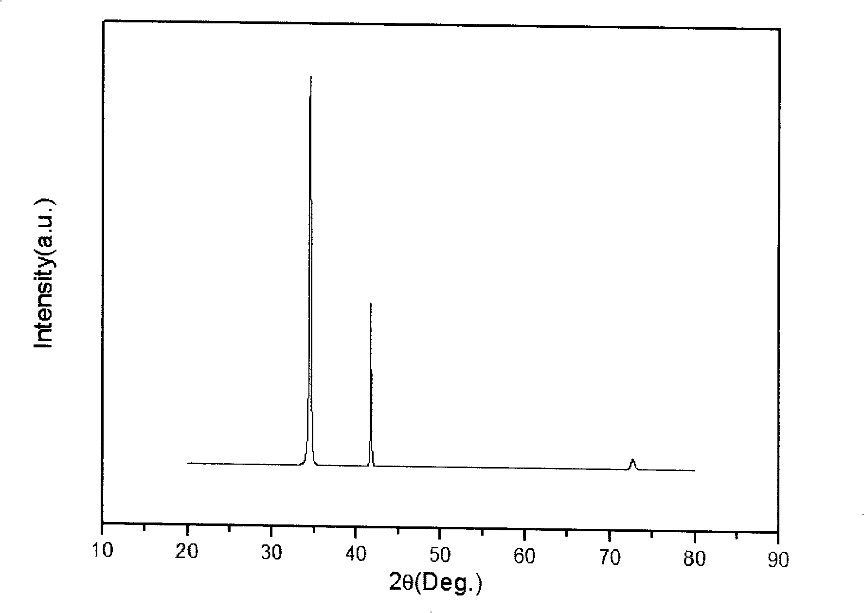

PUM

PropertyMeasurementUnit
Resistivityaaaaaaaaaa
Carrier concentrationaaaaaaaaaa

Abstract

The present invention discloses a method for preparing p type ZnO film by Sb doping, belonging to the field of semiconductor doping technology. The invention relates to a p type Zno doping technology, particularly to a doping technology by metal organic chemical vapor deposition (MOCVD) technology, which uses organic source as the p type doping agent of ZnO. The method is characterized in: with antimony metallorganic as the doping source of p type ZnO, antimony doping p type ZnO film is prepared by metal organic chemical vapor deposition. When the temperature of a substrate is 250 DEG to 650 DEG C, the proportion of antimony doping to ZnO is controlled by adjusting the carrier gas flow rate of antimony metallorganic and zinc metallorganic to grow p type ZnO. The effect and benefit of the invention lies in a high-quality high-controllability p type ZnO growing technology is provided, which is an industrial production transplantable metal organic chemical vapor deposition technology, the difficulty of p type ZnO doping is overcome, thus to realize p-n junction type optoelectronic devices of ZnO.

Description

technical field [0001] The present invention relates to the doping technology of p-type ZnO, the method for growing p-type ZnO film by Sb doping, belongs to the technical field of semiconductor materials, in particular to a kind of p-type ZnO which adopts metal organic chemical vapor deposition (MOCVD) technology and uses organic source as ZnO Doping method of dopant. Background technique [0002] ZnO is another new type of wide bandgap semiconductor material after GaN, which has higher exciton binding energy than GaN material, and can achieve efficient exciton-related emission at room temperature or even higher temperature. However, in order to realize the application in optoelectronic devices, the p-type doping of ZnO has always been a research hotspot. Because there are many intrinsic defects in ZnO, such as Zn gaps, O vacancies, etc., making undoped ZnO an n-type semiconductor material, and these defects have a strong self-compensation effect, so it is difficult to do p...

Claims


Application Information

Patent Timeline
IPC IPC(8): C23C16/40C23C16/455C23C16/52
Inventor 梁红伟杜国同赵涧泽孙景昌边继明胡礼中
Owner DALIAN UNIV OF TECH
Why Eureka
Try Eureka