Miniature array spectral filter based on metallic surface plasma excimer
A technology of plasmons and microarrays, which is applied in the direction of optical filters, can solve the problem of single application range, and achieve the effects of wide material selection, simple process flow, and easy integration
- Summary
- Abstract
- Description
- Claims
- Application Information
AI Technical Summary
Problems solved by technology
Method used
Image
Examples
Embodiment 1
[0016] Example 1. Microarray filter based on area normalized transmission enhancement under normal incidence of P polarized light
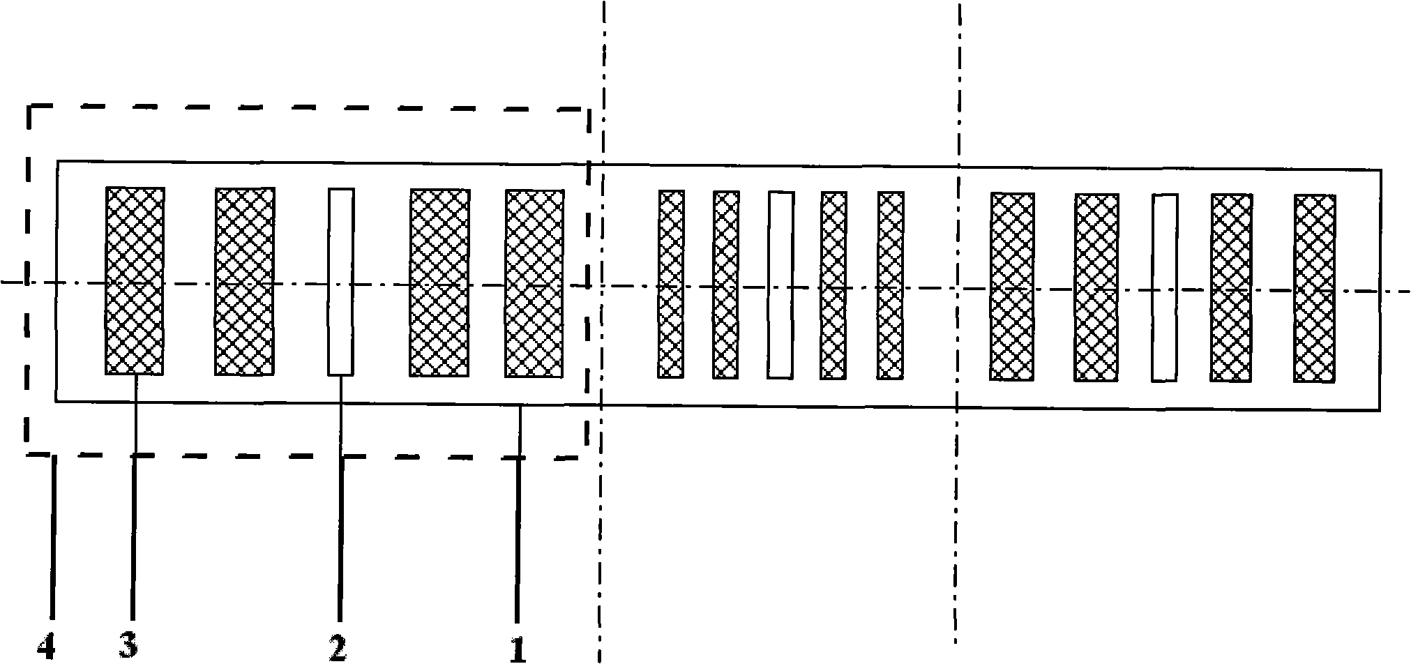
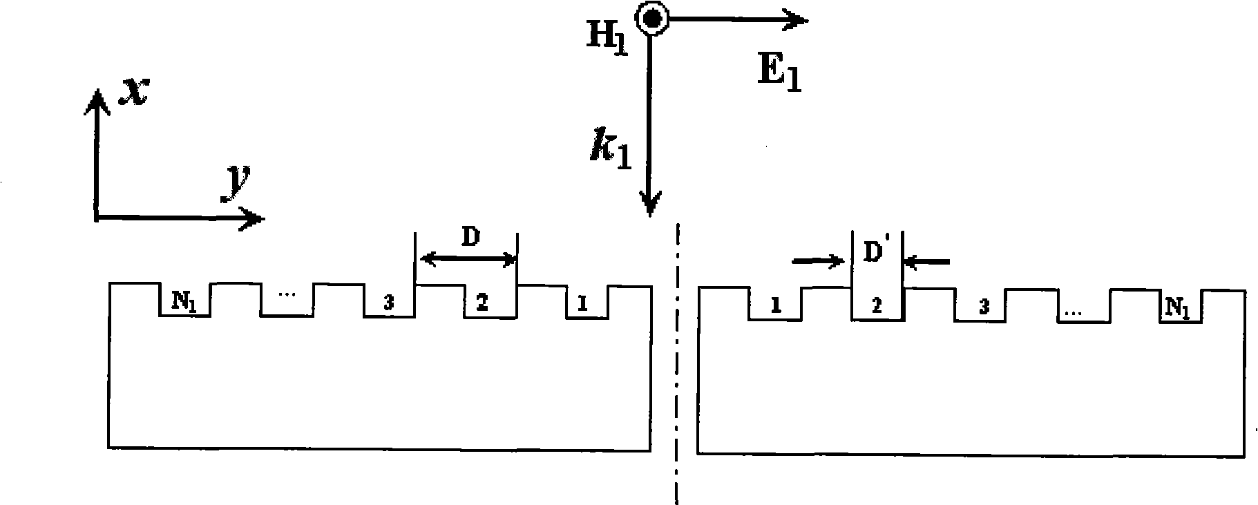
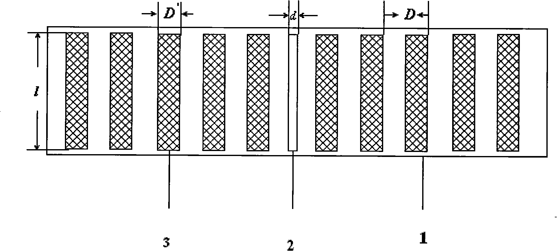
[0017] Normal blue LED wavelength λ 1 =465±5nm, green LED wavelength λ 2 =520±5nm, red LED wavelength λ 3 =630±5nm, combined with the reference wavelength, the structure diagram of the micro-array filter is as follows figure 1 As shown, metal silver (Ag) is selected as the optical substrate material, and a subwavelength slit is arranged in the middle of each array unit, and 5 linear grid grooves symmetrically distributed on the incident surface are arranged at intervals on both sides of the subwavelength slit , the spacing of the linear grid grooves is the same as the width of the linear grid grooves. The transmissive cell structures are available in three different sizes, enabling the realization of transmission-enhancing filters based on the incident wavelengths of red, green and blue. figure 1 Select the width of the mid-subwavelength slit ...
Embodiment 2
[0018] Example 2. Transmission enhancement and beam converging device combining sub-wavelength slits and linear grid grooves under the condition of normal incidence of P polarized light
[0019] Transmission structural units such as Figure 5 As shown, metal silver (Ag) is selected as the optical substrate material, a subwavelength slit is arranged in the middle of each array unit, and five symmetrically distributed linear beams with both entrance and exit surfaces are arranged at intervals on both sides of the subwavelength slit. Grid grooves, the spacing of the linear grid grooves is the same as the width of the linear grid grooves. The grating groove period of the incident surface D in =600nm, that is, the width of the grid groove is D' in =300nm, the periods of the grid grooves on both sides of the exit surface are: D out1 = 720nm and D out2 =420nm, that is, the width of the grid grooves is: D' out1 =360nm,D out2 =210nm, the depth of each grid groove is h=80nm. The ...
PUM
| Property | Measurement | Unit |
|---|---|---|
| Thickness | aaaaa | aaaaa |
Abstract
Description
Claims
Application Information


