Field effect transistor using amorphous oxide film as channel layer, manufacturing method of field effect transistor using amorphous oxide film as channel layer, and manufacturing method of amorphous

A field effect transistor, amorphous oxide technology, applied in transistors and other directions, can solve problems such as reducing the image quality of display devices

Active Publication Date: 2008-09-03
CANON KK
View PDF2 Cites 159 Cited by
  • Summary
  • Abstract
  • Description
  • Claims
  • Application Information

AI Technical Summary

Problems solved by technology

[0013] When the above-mentioned TFT is used in, for example, a pixel circuit of a display device, the occurrence of the hysteresis phenomenon as described above causes fluctuations in the operation of organic LEDs, liquid crystals, etc. to be driven, and as a result, lowers the image quality of the display device

Method used


Image

  • Field effect transistor using amorphous oxide film as channel layer, manufacturing method of field effect transistor using amorphous oxide film as channel layer, and manufacturing method of amorphous
  • Field effect transistor using amorphous oxide film as channel layer, manufacturing method of field effect transistor using amorphous oxide film as channel layer, and manufacturing method of amorphous
  • Field effect transistor using amorphous oxide film as channel layer, manufacturing method of field effect transistor using amorphous oxide film as channel layer, and manufacturing method of amorphous

Examples


example 1

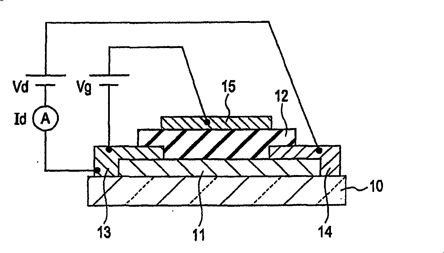
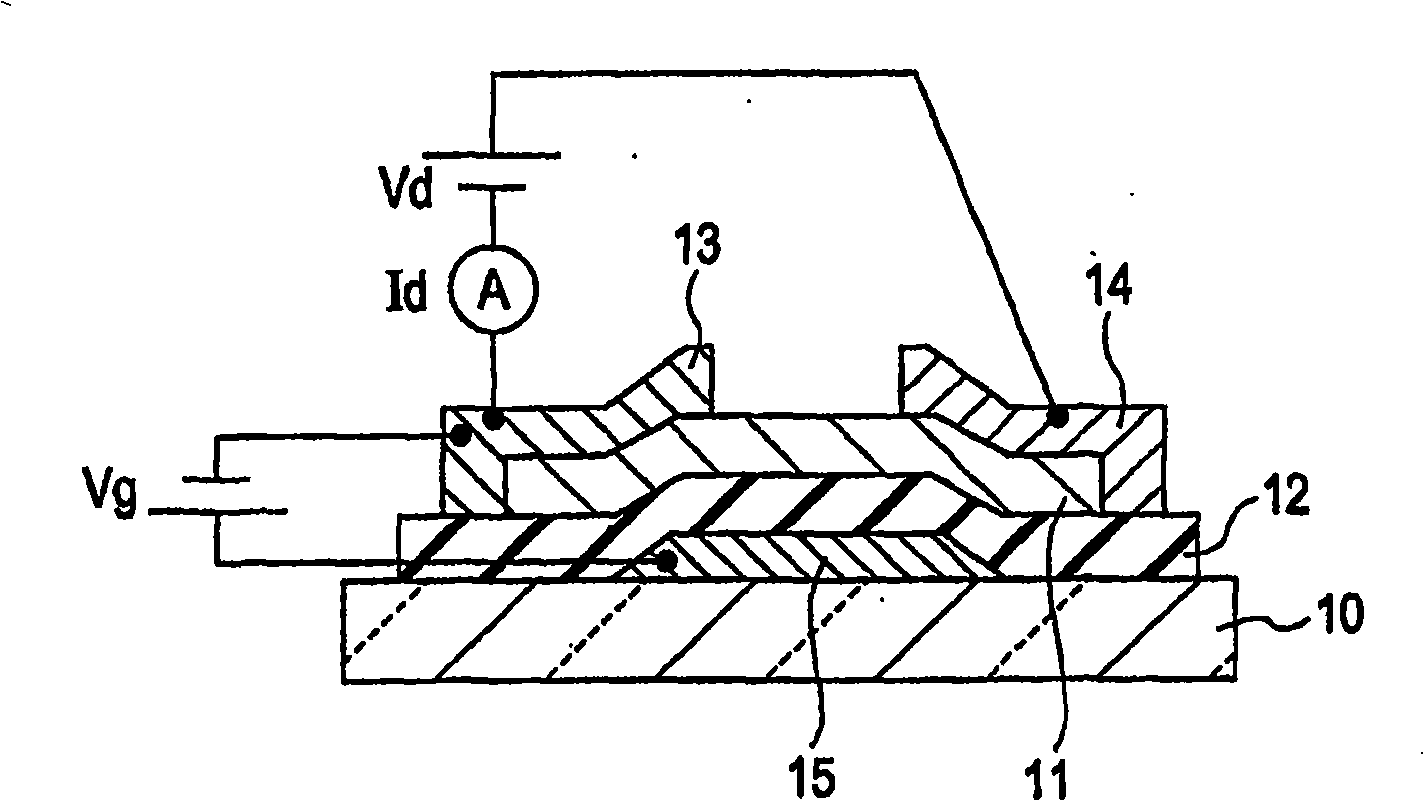
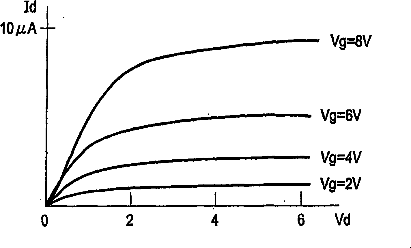
[0103] In this example, the Figure 1A The top-gate TFT shown in . In this example, the channel layer is an In-Ga-Zn-O-based amorphous oxide formed by a sputtering method in a hydrogen-containing gas atmosphere.

[0104] First, an amorphous oxide film containing hydrogen was formed as a channel layer on a glass substrate (Corning #1737 glass produced by Corning Corporation).

[0105] In this example, an In-Ga-Zn-O-based amorphous oxide film containing hydrogen was formed by high-frequency sputtering in a mixed gas atmosphere containing argon, oxygen, and hydrogen.

[0106] use as Figure 5 The sputtering device shown. In this drawing, reference numeral 51 denotes a sample, reference numeral 52 denotes a target, reference numeral 53 denotes a vacuum pump, reference numeral 54 denotes a vacuum gauge, reference numeral 55 denotes a substrate holder, and reference numeral 56 denotes a A gas flow rate controller provided for each gas introduction system, reference numeral 57 den...

example 2

[0133] In this example, an amorphous oxide film containing hydrogen to be used for a channel layer of a thin film transistor will be described. First, an insulating film of amorphous oxide is formed on a quartz substrate.

[0134] The film-forming method of the amorphous oxide was performed in accordance with the film-forming method described in Example 1. Target (material source) is InGaO 3 (ZnO), and the total pressure in the gas environment during film formation is 0.3Pa. In this step, the gas flow ratio is set as Ar:O 2 =95:5, thus the partial pressure of oxygen corresponds to 0.015Pa. In addition, hydrogen gas was not provided. The film thickness was set to about 400 nm. When the resistance of the thin film thus formed was measured by the four-probe method, the electric conductivity was not greater than the measurement limit (0.0001 S / cm or less), and thus it was confirmed that the thin film was an insulating film.

[0135] Next, hydrogen ion implantation was perfor...

example 3

[0143] In this example, the Figure 1A The top-gate TFT shown in . In this case, an amorphous oxide containing hydrogen (or deuterium) was formed by ion-implanting hydrogen or deuterium into an In-Ga-Zn-O-based amorphous oxide formed by a pulsed laser deposition method (PLD method). channel layer.

[0144] First, an In-Zn-Ga-O-based amorphous oxide film was formed on a glass substrate (Corning #1737 glass produced by Corning Corporation) by the PLD method.

[0145] InGaO 3 (ZnO) 4 A polycrystalline sintered material was used as a target, and an In-Zn-Ga-O-based amorphous oxide film was deposited. The oxygen partial pressure during film formation was 7 Pa. The power of the KrF excimer laser is 1.5×10 -3 mJ / cm 2 / pulse, the pulse width is 20 ns, and the repetition rate is 10 Hz. In addition, the substrate temperature was not heated and kept at room temperature of about 25°C.

[0146] According to the results of fluorescent x-ray (XRF) analysis, the metal composition rati...


PUM


Abstract

An amorphous oxide containing hydrogen (or deuterium) is applied to a channel layer of a transistor. Accordingly, a thin film transistor having superior TFT properties can be realized, the superior TFT properties including a small hysteresis, normally OFF operation, a high ON/OFF ratio, a high saturated current, and the like. Furthermore, as a method for manufacturing a channel layer made of an amorphous oxide, film formation is performed in an atmosphere containing a hydrogen gas and an oxygen gas, so that the carrier concentration of the amorphous oxide can be controlled.

Description

technical field [0001] The present invention relates to a field effect transistor having a channel layer formed of an amorphous oxide and having transistor characteristics suitable for display devices and the like. Background technique [0002] A field effect transistor (hereinafter sometimes referred to as "FET") has a gate electrode, a source electrode, and a drain electrode. In addition, a field effect transistor is an active device in which a current flowing in a channel layer, that is, a current flowing between a source electrode and a drain electrode is controlled by applying a voltage to a gate electrode. Specifically, a FET using a thin film formed on an insulating substrate of ceramics, glass, or plastic as a channel layer is called a thin film transistor (hereinafter sometimes referred to as "TFT"). [0003] TFTs can be advantageously and easily formed on relatively large substrates by using thin film forming techniques, and as a result, TFTs have been widely used...

Claims


Application Information

Patent Timeline
Patent Type & Authority Applications(China)
IPC IPC(8): H01L29/786
Inventor 岩崎达哉
Owner CANON KK
Why Eureka
Try Eureka