A tube phase change memory unit structure and its making method

A technology of phase-change memory and cell structure, which is applied in the field of microelectronics and can solve the problems of large peripheral circuits, large operating current, and large power consumption.

Active Publication Date: 2008-09-17
SHANGHAI INST OF MICROSYSTEM & INFORMATION TECH CHINESE ACAD OF SCI
View PDF1 Cites 26 Cited by
  • Summary
  • Abstract
  • Description
  • Claims
  • Application Information

AI Technical Summary

Problems solved by technology

The contact area between the phase-change material and the lower electrode is determined by the cross-sectional area of ​​the lower electrode. The width of the lower electrode depends on the photolithography pattern defined by the photolithography process. The minimum width of the bottom electrode depends on the minimum width of the photolithography process. The structure is shrinking The cross-sectional area of ​​phase change materials is limited by the current photolithography process and conditions
[0005] The current problem in the phase change memory cell structure is that the operation current required from the crystalline state to the amorphous state is large, resulting in large peripheral circuits and high power consumption

Method used


Image

  • A tube phase change memory unit structure and its making method
  • A tube phase change memory unit structure and its making method
  • A tube phase change memory unit structure and its making method

Examples


Embodiment Construction

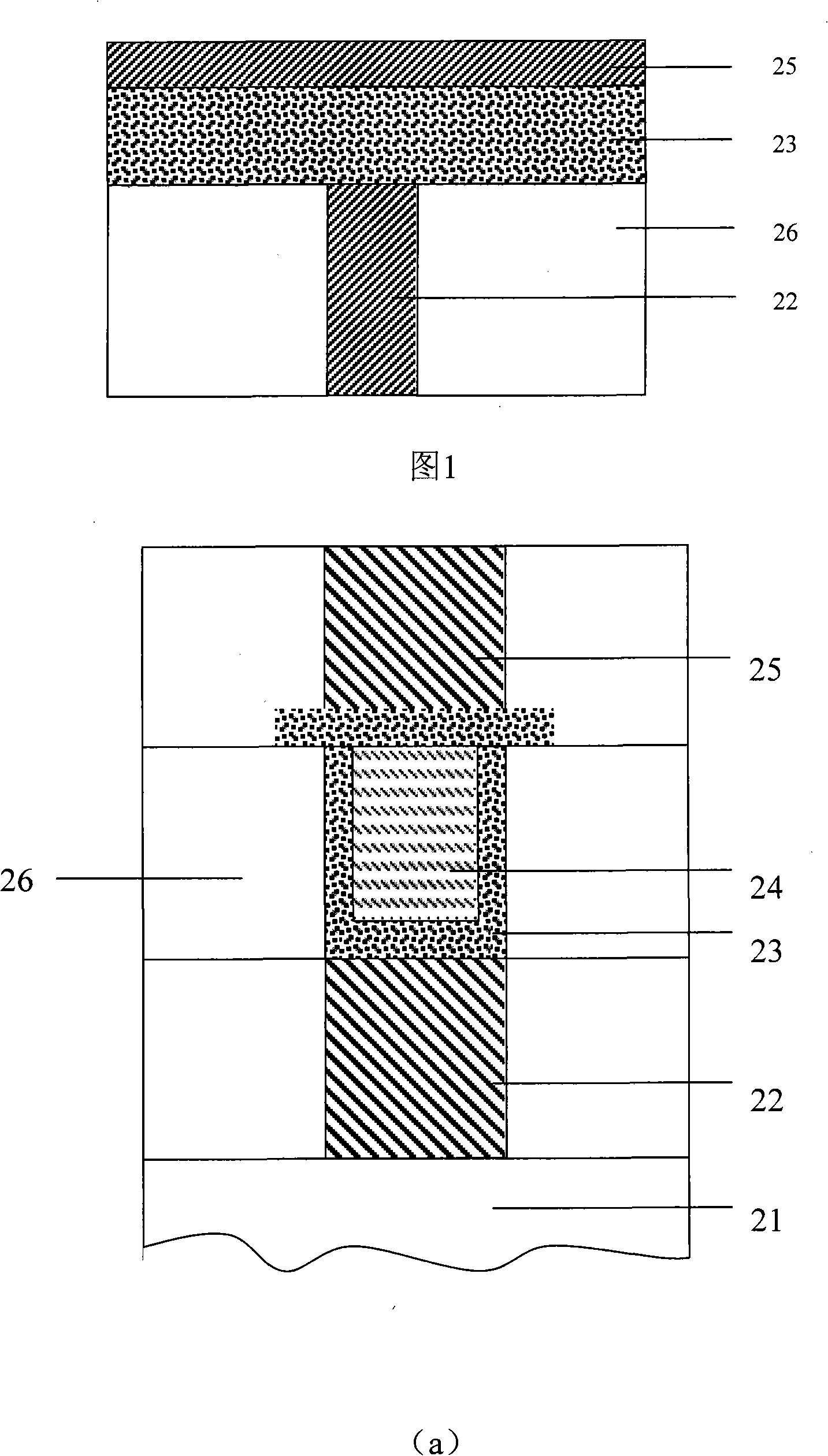
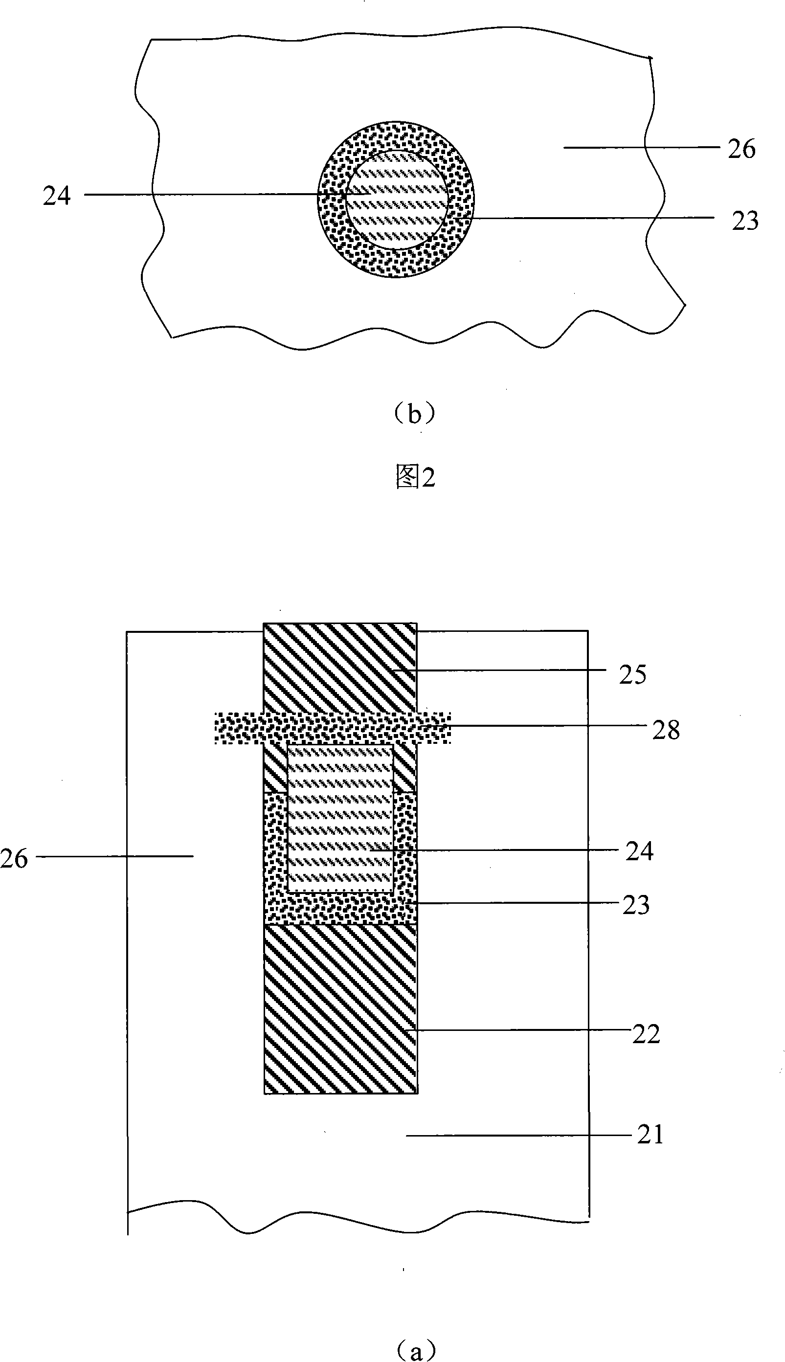
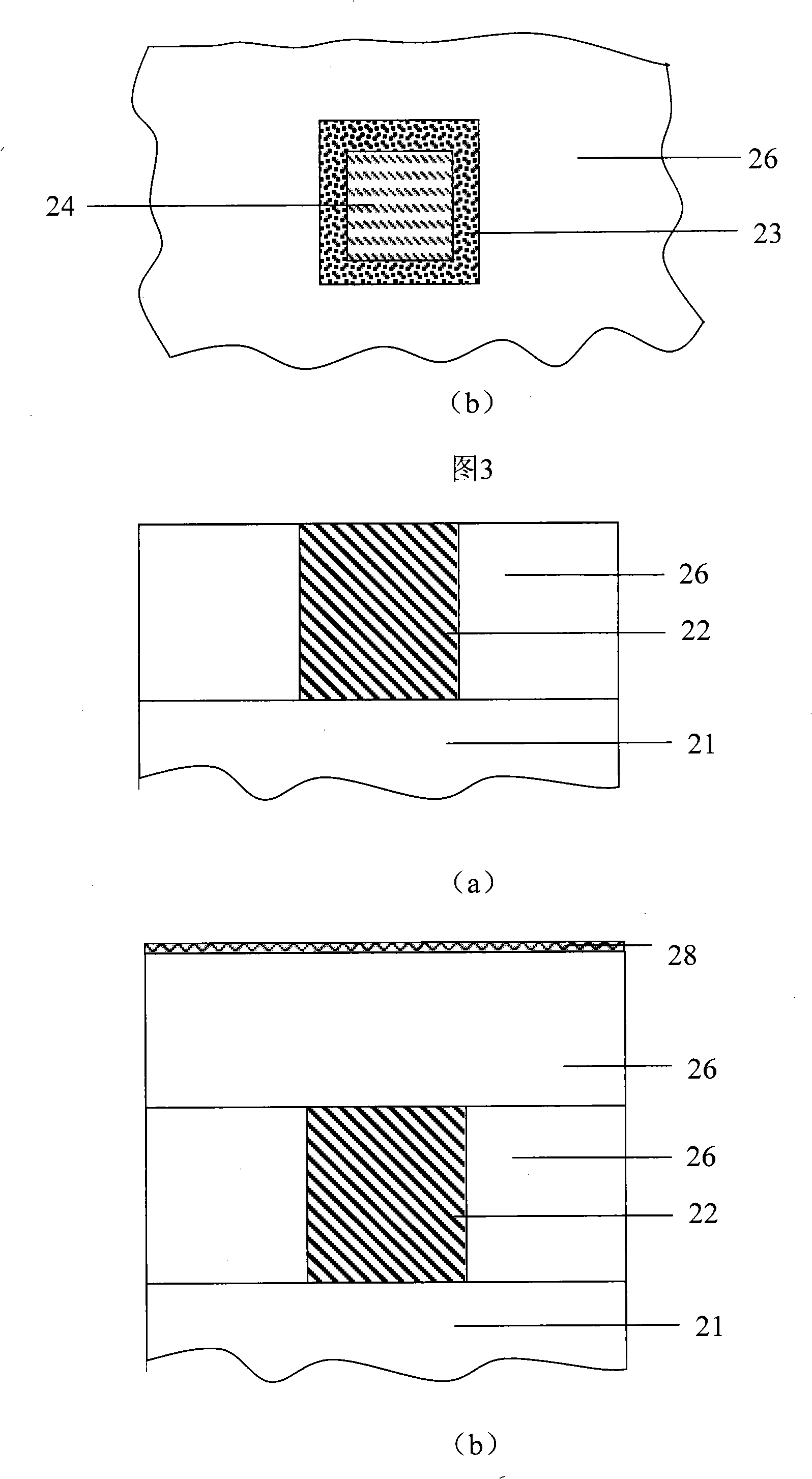
[0018] The invention is described more fully below with reference to the drawings, which provide preferred embodiments but should not be considered limited to the embodiments set forth herein. In the drawings, the thicknesses of layers and regions are exaggerated for clarity, but as schematic diagrams, they should not be considered as strictly reflecting the proportional relationship of geometric dimensions. Here, the referenced figures are schematic views of the present invention, and the representations in the figures are schematic, but should not be considered as limiting the scope of the present invention.

[0019]Figure 4 (a)-(f) illustrate methods of forming certain embodiments of the present invention. The following is a further introduction to the operation steps of preparing this ring-shaped phase-change memory unit in combination with the diagrams:

[0020] 1. If Figure 4 (a) As shown in the substrate (including the MOS impurity diffusion region, source and drain r...


PUM


Abstract

The invention relates to a tube-like phase-change memory single structure and making method, the phase-change memory single structure comprises a top electrode, a bottom electrode and a memory part. The single structure has basic characters that: phase-change material distributes at lateral wall of a hole, the phase-change is implemented in the hole in reading and writing operation through heating own by using small sectional area and big resistance of the phase-change material, and tubular is formed at two ends of ring phase-change material through adding phase-change material insulating layer as closure, thus improving use efficiency of heat in the reading and writing operation, the memory part is a tubular structure enclosed by the phase-change material up and down, and is filled with metal, insulation materials or high resistivity material. The memory structure of the invention can reduce operating current, and has small-power, high heat utilization ratio and good data retention performance, and the invention can improve the consistency of resistance value of device of chip.

Description

technical field [0001] The invention relates to a semiconductor device and a manufacturing method thereof, in particular to a tubular phase-change memory device unit structure and a manufacturing method, belonging to the technical field of microelectronics. Background technique [0002] Memory occupies an important position in the semiconductor market. Only DRAM (Dynamnic Random Access Memory) and FLASH occupy 15% of the entire market. With the gradual popularization of portable electronic devices, the market for non-volatile memory is also growing. At present, FLASH It accounts for the mainstream of non-volatile memory, accounting for about 90%. However, with the advancement of semiconductor technology, FLASH has encountered more and more technical bottlenecks. First, the floating gate for storing charges cannot be thinned indefinitely with the development of integrated circuit technology. In addition, other shortcomings of FLASH technology also limit Its application, such...

Claims


Application Information

Patent Timeline
Patent Type & Authority Applications(China)
IPC IPC(8): H01L45/00H01L27/24H01L21/82G11C11/56G11C16/02
Inventor 凌云宋志棠封松林
Owner SHANGHAI INST OF MICROSYSTEM & INFORMATION TECH CHINESE ACAD OF SCI
Why Eureka
Try Eureka