

Radiation curable thermal transfer elements
A technology of radiation curing and heat transfer, which is applied in the fields of electrical components, electric solid-state devices, and the application of radiation from radioactive sources, and can solve problems such as impracticality and device difficulties.
- Summary
- Abstract
- Description
- Claims
- Application Information
AI Technical Summary
Problems solved by technology
Method used
Image

Examples
example 1
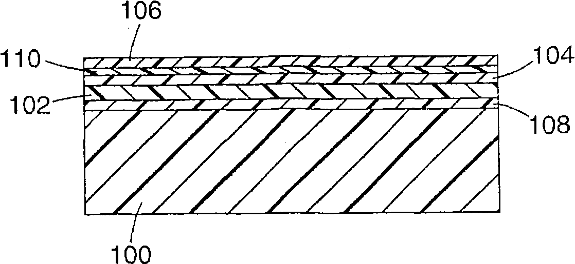
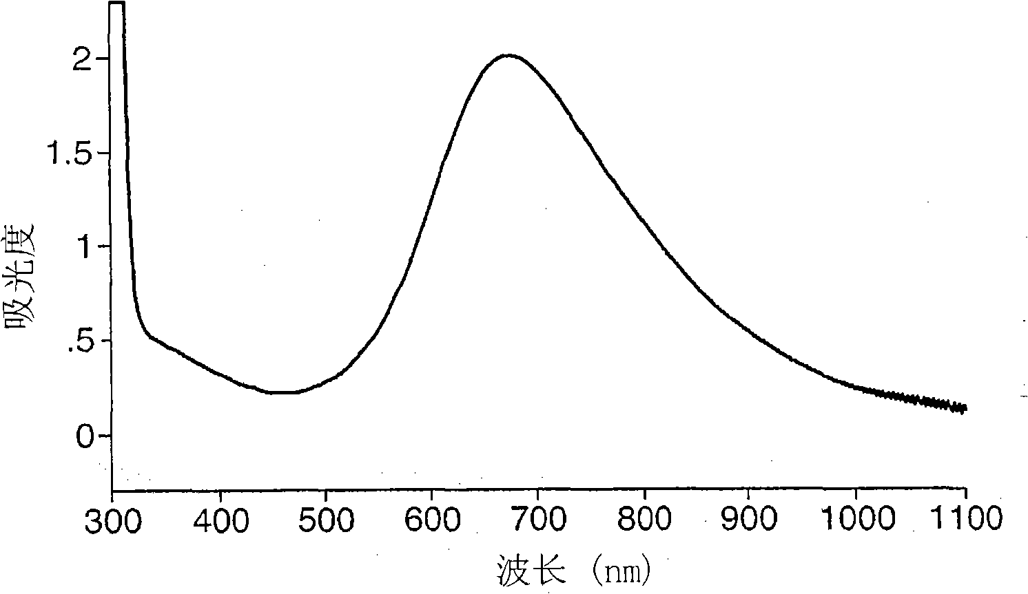
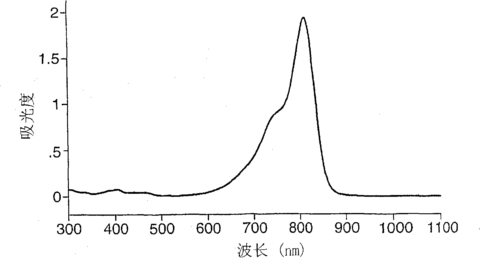
[0127] An LTHC layer comprising carbon black and Prussian blue (also known as iron blue and pigment blue 27) with similar absorption at 808 nm was prepared.
[0128] Sample 1 was prepared in the following manner. Prior to application of the LTHC solution, 2.88 mil thick polyethylene terephthalate (DuPont Teijin Films, Hopewell VA) was tested using nitrogen gas at 300 watts and a line speed of 50 ft / min. The inside of the M7Q base film substrate is corona treated. A Prussian blue-based LTHC solution (non-particulate absorbing material) containing the components shown in Table I was then applied to the corona-treated processed M7Q film. To achieve a dry thickness of approximately 2.8 microns, a line speed of 20 ft / min and a 180R microgravure printing mode set at 9.0 ft / min were used. The coatings were sequentially passed into three ovens (75 / 75 / 80° C.) for in-line drying, and then dried under a 600 W / inch lamp (with a D bulb set at 70% power) by Fusion UV Systems, Inc. (Gaith...
example 2
[0136] A series of LTHC layer coatings with different pigment loadings were prepared according to the components shown in Table IV.
[0137]Sample 5 was prepared in the following manner. Prior to application of the LTHC solution, 2.88 mil thick polyethylene terephthalate (DuPont Teijin Films, Hopewell VA) was tested using nitrogen gas at 300 watts and a line speed of 50 ft / min. The inside of the M7Q base film substrate is corona treated. A Prussian blue-based LTHC solution prepared with 9S928D (non-particulate absorbent) containing the components shown in Table IV was then applied to the corona-treated M7Q film. The LTHC solution was applied using reverse micro-gravure coating (Yasui Seiki laboratory coater, model CAG-150). To achieve a dry thickness of approximately 1.25 microns, a line speed of 20 ft / min and a 200R microgravure printing mode set at 6.2 ft / min were used. The coating sequentially enters three ovens (75 / 75 / 80° C.) for in-line drying, and is then exposed to u...
example 3
[0147] The emissive layer of the OLED device was patterned using a Prussian blue LITI donor film as previously described in Example 2, Sample 7, comprising a radiation-cured thermal transfer element comprising 21.6% Pigment loading of Prussian blue pigment dispersed in 2.75 μm thick LTHC as imaging radiation absorbing material.
[0148] Receptor substrates were prepared on glass (0.7 mm thick) coated with ITO available from ULVAC Technologies, Inc. (Methuen, MA) under the trade designation S-ITO (150 NM). The substrate was spin coated with a Baytron P VP CH8000 (H.C. Starck Co., Newton, MA) to a dry thickness of approximately 60 nm and then heated to 200° C. for 5 minutes in a nitrogen purged oven. The coated HTM-001 (a hole-transporting polymer from Covion Organic Semiconductors GmbH (Frankfurt, Germany)) and toluene solution were then used to place it in an argon-purged glove box. The substrate was spin-coated to a dry thickness of approximately 100 nm. Finally, use standa...
PUM
| Property | Measurement | Unit |
|---|---|---|
| thickness | aaaaa | aaaaa |
| thickness | aaaaa | aaaaa |
| thickness | aaaaa | aaaaa |
Abstract
Description
Claims
Application Information