Extension method of material for low forward voltage drop Schottky diode

A technology of Schottky diode and forward voltage drop, which is applied in the direction of electrical components, semiconductor/solid-state device manufacturing, circuits, etc., can solve the problems of high forward voltage drop, reduction of effective thickness of epitaxy, poor repeatability and reproducibility, etc. achieve low forward voltage drop

Active Publication Date: 2008-10-29
HEBEI POSHING ELECTRONICS TECH
View PDF0 Cites 10 Cited by
  • Summary
  • Abstract
  • Description
  • Claims
  • Application Information

AI Technical Summary

Problems solved by technology

The active area mainly comes from the epitaxial layer of the material used in Schottky diodes. Under ordinary processes, the normal growth transition area is generally greater than 1.3 microns, the uniformity of resistivity in the chip is greater than 7%, and the uniformity of resistivity in the furnace is greater than 10%. , and the repeatability and reproducibility between furnaces are poor. Using this material to manufacture Schottky diodes, when the reverse breakdown voltage meets the requirements, because the transition zone is longer, the corresponding epitaxial effective thickness is reduced, so more Large total epitaxial thickness, resulting in excessive forward voltage drop

Method used


Image

  • Extension method of material for low forward voltage drop Schottky diode
  • Extension method of material for low forward voltage drop Schottky diode

Examples


Embodiment Construction

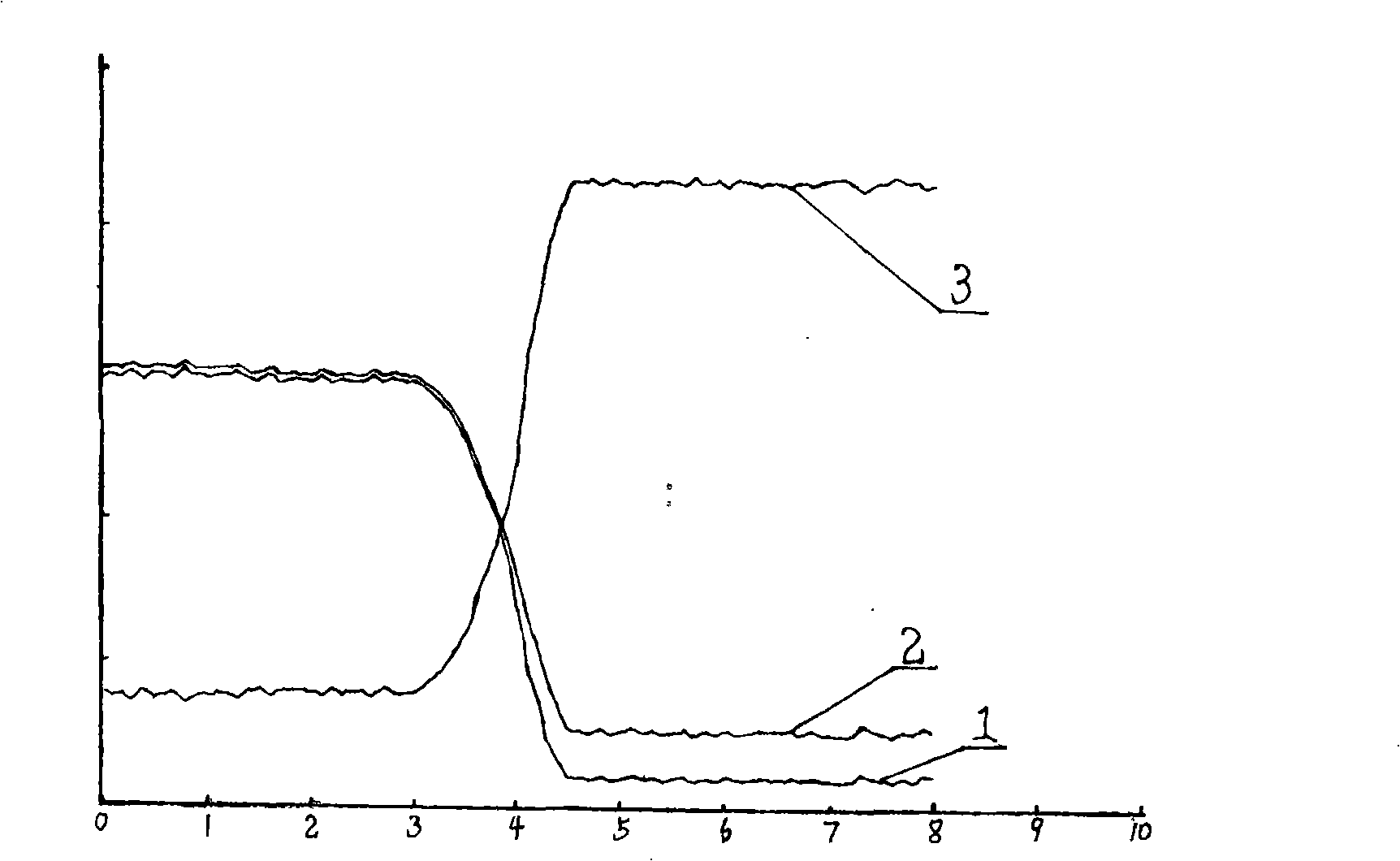
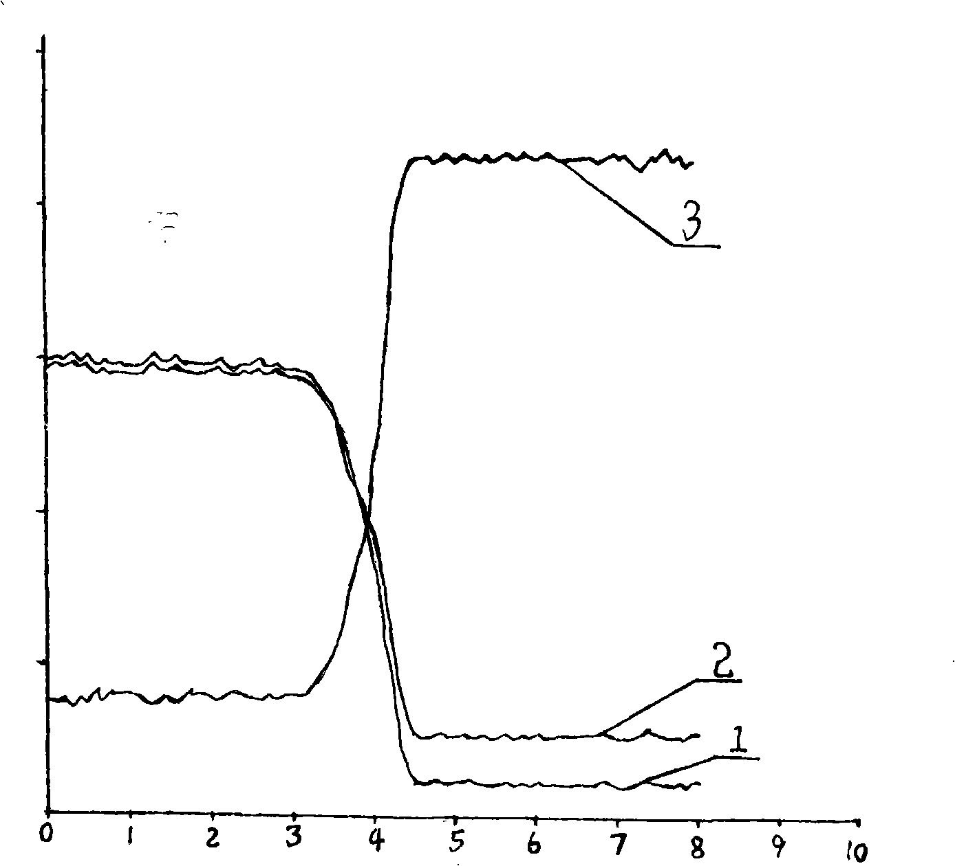
[0030] Below in conjunction with experimental result the present invention is described in further detail:

[0031] 1. Put the substrate into the reaction chamber, first use nitrogen gas for 3 minutes, then turn off the nitrogen gas, and then use hydrogen gas (the hydrogen valve is opened to the maximum) to drive nitrogen gas for 4 minutes;

[0032] 2. Reduce the hydrogen flow rate to 60-150 liters per minute, such as the usual 100 liters per minute, and raise the temperature of the reaction chamber from room temperature to 650 degrees in 5 minutes, and from 650 degrees to 900 degrees in 10 minutes. It takes 8 minutes to rise from 900 degrees to 1150 degrees, and it takes 6 minutes to raise the temperature from 1150 degrees to 1190 degrees, such as a typical 1160 degrees. During the process of rising from 1150 degrees to 1190 degrees, increase the hydrogen flow to 180-220 L / min, such as the usual 200 liters / min, while feeding HCl to get rid of gas;

[0033] 3. After heating u...


PUM


Abstract

The invention discloses an extension method for a material used for a lower positive pressure reduction schottky diode. The invention controls and optimizes the temperature rising time of each step by adjusting the program of temperature rising and the careful cooperation of hydrogen flux to lead the impurities of a wafer from an underlay to be expanded outwards during a heat treatment process and finally lead the transition area of a silicon epitaxial wafer to reach the range of 1.2 to 1.3 micron by expelling the air by hydrogen. The resistance rate uniformity in the wafer is less than 3 percent by adopting the method of the invention, thereby leading the transition area of the wafer to be controlled between 1.0 and 1.3 micron and leading the resistance rate uniformity in a furnace to be less than 5 percent; besides, the repetitiveness and the reproducibility of the resistance rate and the thickness between furnaces are good; the repetitiveness in the furnace and the transition area of the wafer is good; the uniformity and the consistency of the positive pressure reduction and negative pressure reduction of the schottky diode manufactured by the material are good.

Description

technical field [0001] The invention relates to an epitaxy method for materials for Schottky diodes, in particular to an epitaxy method for materials for low forward voltage drop Schottky diodes. Background technique [0002] For a diode, its power consumption depends on the diode current If and the forward voltage drop Vf. Since If is predetermined by the application, the only way to reduce the power consumption of the diode is to reduce the forward voltage drop (VF). For Schottky rectifier diodes, the forward voltage drop Vf depends on the metal barrier layer and active area used by the diode. The active area mainly comes from the epitaxial layer of the material used in Schottky diodes. Under ordinary processes, the normal growth transition area is generally greater than 1.3 microns, the uniformity of resistivity in the chip is greater than 7%, and the uniformity of resistivity in the furnace is greater than 10%. , and the repeatability and reproducibility between furnace...

Claims


Application Information

Patent Timeline
Patent Type & Authority Applications(China)
IPC IPC(8): H01L21/02H01L21/20H01L21/329
Inventor 赵丽霞袁肇耿
Owner HEBEI POSHING ELECTRONICS TECH
Why Eureka
Try Eureka