Technological process for transferring film by means of sacrificial layer

A technology of film transfer and process method, which is applied in the process of producing decorative surface effects, metal material coating process, coating and other directions, can solve the problem of incomplete compatibility between heat-sensitive film and micro-bridge structure process, and achieve a It is beneficial to large-scale production and the method is simple and easy to implement.

Inactive Publication Date: 2008-11-05
SHANGHAI INST OF TECHNICAL PHYSICS - CHINESE ACAD OF SCI
View PDF0 Cites 5 Cited by
  • Summary
  • Abstract
  • Description
  • Claims
  • Application Information

AI Technical Summary

Problems solved by technology

[0005] The purpose of the present invention is to provide a simple, fast and effective method of film transfer using a sacrificial layer to transfer a large-scale microbridge

Method used


Image

  • Technological process for transferring film by means of sacrificial layer

Examples


Example Embodiment

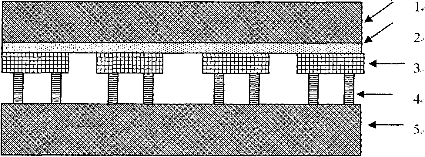
[0016] In this embodiment, the substrate 1 of the microbridge array is made of bonded glass, the sacrificial layer 2 is made of polyimide, and the interconnection column 4 is made of indium column.

[0017] The following are the concrete steps of utilizing the film transfer of the present invention:

[0018] (1) Polyimide (thickness 5 μm) was spin-coated as a sacrificial layer on a bonded glass substrate, imidized (400° C., 1 hour, nitrogen protection), and a microbridge array was prepared thereon.

[0019] (2) Indium pillars (10 μm in diameter and 10 μm in height) are prepared on the microbridge array and the readout circuit respectively by a lift-off process, and the microbridge array substrate is turned over to align with the readout circuit and interconnected.

[0020] (3) The polyimide ashing method (segmented etching, temperature control of the substrate, about two hours in total) using oxygen plasma to directly separate the glass substrate.


PUM


Abstract

The invention discloses a technique method for transferring a film by utilizing a sacrificial layer. The specific technique method comprises the following steps: a sacrificial layer is firstly coated on the substrate of a microbridge array, then the microbridge array is prepared on the sacrificial layer, after that, a reading circuit and the microbridge array are reversed and inter-connected, finally, the sacrificial layer is removed and the substrate of the microbridge array is separated automatically. The method can avoid the chip protection and end point monitoring problem during the process of removing the substrate of the microbridge array, and can realize the large-scale transfer of the microbridge array in a rapid and efficient way.

Description

technical field [0001] The invention belongs to the technical field of microfabrication of detectors, and specifically refers to a process method for film transfer using a sacrificial layer. It is suitable for making hybrid large-scale uncooled focal plane arrays, and is also suitable for all applications that require large-scale overhead film arrays. device. Background technique [0002] The uncooled focal plane is essentially a "thermal" detector, which uses the "radiant heat effect" of the sensitive element for infrared detection. Its core is an infrared sensitive element array with a certain heat accumulation ability and thermal effect. [0003] The uncooled focal planes of microbolometers developed by major foreign R&D institutions and companies generally use CMOS readout circuits, vanadium oxide or polysilicon as heat-sensitive films, and technical solutions for monolithic integration of focal plane microbridge arrays and CMOS readout circuits. . However, the process...

Claims


Application Information

Patent Timeline
IPC IPC(8): B81C1/00
Inventor 程正喜马斌翟厚明施永明张学敏
Owner SHANGHAI INST OF TECHNICAL PHYSICS - CHINESE ACAD OF SCI
Why Eureka
Try Eureka