
Electrolytic ni plating apparatus and method of manufacturing semiconductor device

A device manufacturing method and equipment manufacturing technology, applied in semiconductor/solid-state device manufacturing, semiconductor devices, electric solid-state devices, etc., can solve problems such as reduced film formation rate, reduced current efficiency, not passivation problems, etc., to prevent current Decrease in efficiency and film formation rate, effect of suppressing passivation

Inactive Publication Date: 2008-11-19
NEC ELECTRONICS CORP
View PDF2 Cites 9 Cited by
  • Summary
  • Abstract
  • Description
  • Claims
  • Application Information

AI Technical Summary

Problems solved by technology

Therefore, for the case of continuously performing the wafer under the condition of a large current density, in other words, for the case of keeping the nickel anode 105 at a high potential for a long duration, there is a problem that the surface of the nickel anode 105 is damaged. Passivation, so that the current efficiency decreases, and the film formation rate also decreases
However, the goal of this technique is not to solve the passivation problem

Method used


Image

  • Electrolytic ni plating apparatus and method of manufacturing semiconductor device
  • Electrolytic ni plating apparatus and method of manufacturing semiconductor device
  • Electrolytic ni plating apparatus and method of manufacturing semiconductor device

Examples


example 1

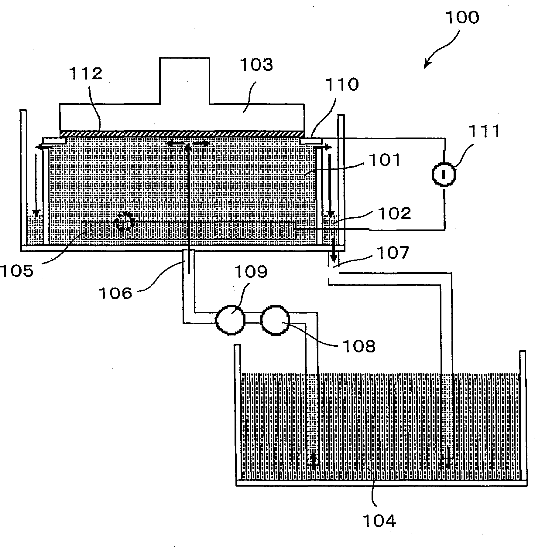
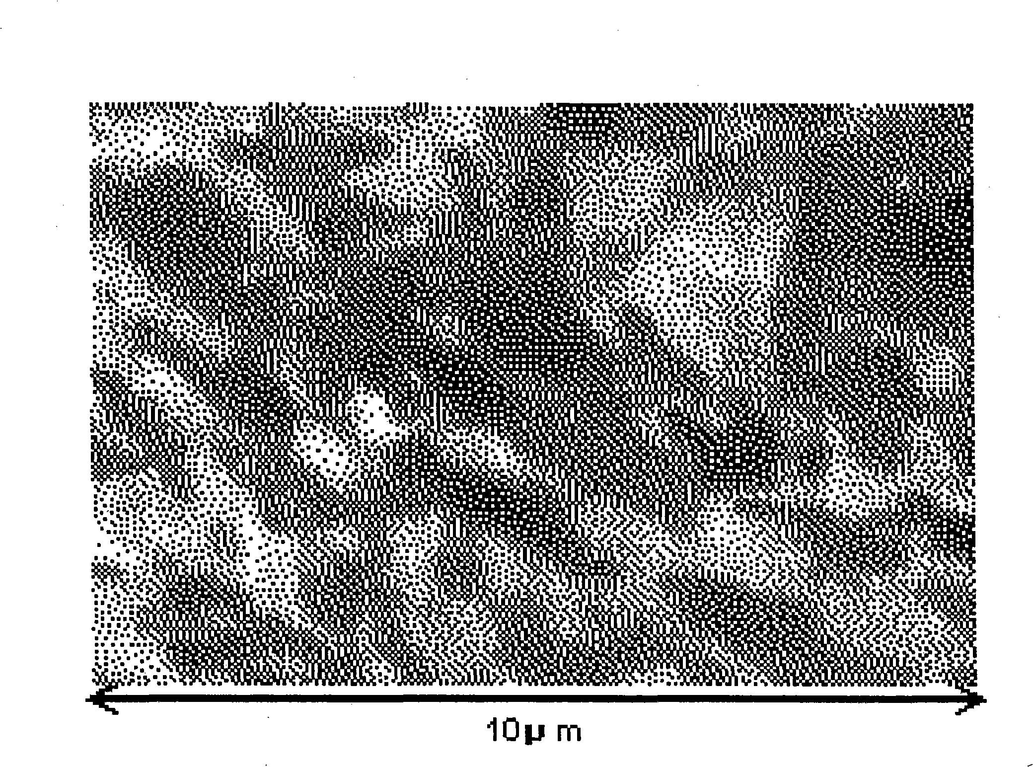
[0035]Wafers were continuously processed at a large current density using an electrolytic nickel plating apparatus provided with a nickel anode having an average grain size of 10 μm or less. The average grain size of the nickel anode is calculated as follows. First, a clean section of the anode is made with a FIB (Focused Ion Beam) device, and then an image of this section is taken with a SIM (Scanning Ion Microscope). image 3 A SIM image of the nickel anode of this example is shown.

[0036] The average grain area S can be obtained by dividing the unit area by the number of grains. In the SIM image of this example, the number of grains per unit area can be counted. The average grain area S is obtained by dividing the unit area by the number of grains counted. Next, the average grain size L was calculated by approximating the grains to a circle in order to convert the area into a length. The average grain size L is calculated by the following formula:

[0037] ...


PUM

PropertyMeasurementUnit
particle sizeaaaaaaaaaa

Abstract

The invention relates to an electrolyzed nickel plating device and method for producing a semiconductor device. The invention aims at providing an electrolyzed nickel plating device which can restrain passivation on the surface of nickel anode, prevent reduction of current efficiency and film forming speed, provide stable nickel plating for improving quality and maintain stable output. The electrolyzed nickel plating device is provided with the nickel (Ni) anode with the average grain size of 10 um or less.

Description

[0001] This application is based on Japanese Patent Application No. 2007-017703, the contents of which are incorporated herein by reference. technical field [0002] The invention relates to electrolytic nickel plating equipment and a manufacturing method of a semiconductor device. Background technique [0003] As an environmental protection measure, lead-free solder has spread rapidly these days. There is currently a tendency to replace the barrier metal from Cu to Ni for lead-free solders suitable for flip-chip products for semiconductor devices. Cu exhibits a larger rate of alloying, while Ni exhibits a smaller rate of alloying. The Ni film is usually formed by electroless plating or electrolytic plating. Beryllium-nickel equipment, especially used in semiconductor manufacturing processes, is required to form nickel-plated thin films in a stable and high-yield manner. In traditional electrolytic plating equipment used in semiconductor manufacturing processes, soluble N...

Claims


Application Information

Patent Timeline
Patent Type & Authority Applications(China)
IPC IPC(8): C25D17/10C25D7/12H01L21/288
CPCH01L24/03H01L2924/01082H01L2924/01004H01L24/13H01L2224/93H01L2224/741H01L24/741H01L2224/03462H01L24/05H01L2924/01033H01L2224/0362H01L2224/13116H01L2924/01006H01L2924/01029H01L2924/01078H01L24/93H01L2224/0401C25D17/10H01L2224/05655H01L2924/014H01L2224/05147H01L2224/03C25D17/00
Inventor 橘裕昭
Owner NEC ELECTRONICS CORP
Learn More