Resistor memory with doping control layer

A resistive memory, resistive memory technology, applied in the field of microelectronics, can solve the problems of difficult control of doping amount, loss of device switching performance, etc.

Inactive Publication Date: 2008-12-03
FUDAN UNIV
View PDF0 Cites 14 Cited by
  • Summary
  • Abstract
  • Description
  • Claims
  • Application Information

AI Technical Summary

Problems solved by technology

The current doping method is to directly contact the doped metal with the storage medium to achieve diffusion doping [1][3] , so the doping method is difficult to control the doping amount, and it is not suitable for metal oxide resistance memory films that only need low doping, for example, Cu x Doping a small amount of Ta on the surface of the O resistance storage layer can improve the power consumption of the device and stabilize the performance of the device, but Ta and Cu x The direct contact of O film with doping will make the Cu x Excessive Ta content in O leads to loss of device switching performance

Method used


Image

  • Resistor memory with doping control layer
  • Resistor memory with doping control layer
  • Resistor memory with doping control layer

Examples


Embodiment Construction

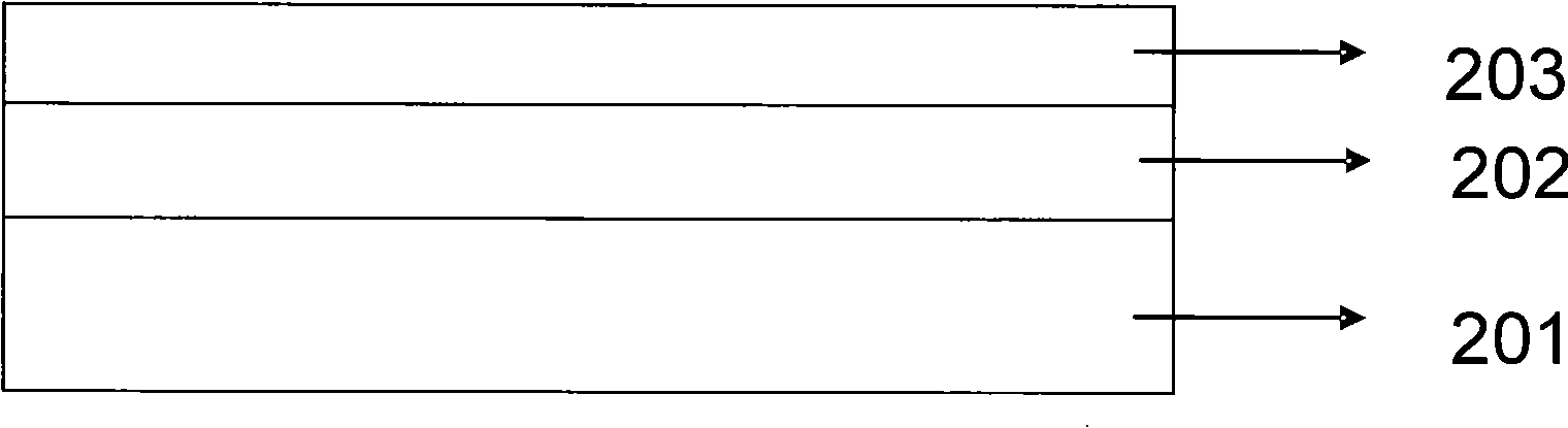
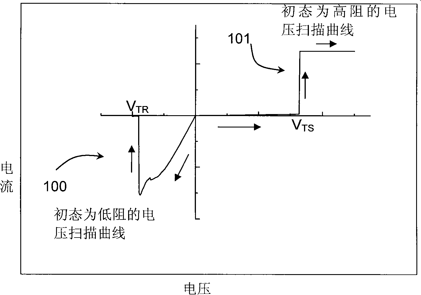
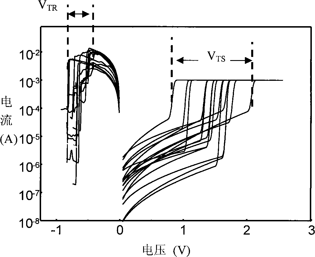
[0033] The invention is described more fully hereinafter in reference to the examples illustrated in the illustrations, providing preferred embodiments but should not be considered limited to the embodiments set forth herein. In the drawings, the thicknesses of layers and regions are exaggerated for clarity, but as schematic diagrams, they should not be considered as strictly reflecting the proportional relationship of geometric dimensions.

[0034] The drawings referenced herein are schematic illustrations of idealized embodiments of the invention, and the illustrated embodiments of the invention should not be considered limited to the particular shapes of the regions shown in the drawings, but include resulting shapes, such as manufacturing-induced deviation. For example, the curves obtained by dry etching usually have curved or rounded characteristics, but in the illustrations of the embodiments of the present invention, they are all represented by rectangles, and the repre...


PUM


Abstract

The invention belongs to the micro-electron technical field, in particular to a resistance memory with a doped control layer. The resistance memory comprises an upper electrode, a lower electrode, a resistance memory medium layer used for realizing the memory conversion of the resistance value, and a doped control layer used for realizing the metal element doping of the resistance memory medium layer and controlling of the doping content. The doped control layer and the resistance memory medium layer are directly connected with each other and the metal element in the upper electrode or the lower electrode penetrates through the doped control layer to diffuse towards the surface of the memory medium layer so as to realize the controllable low doping of the resistance memory medium layer, thus achieving the object of stabilizing the electric performance of the resistance memory.

Description

technical field [0001] The invention belongs to the technical field of microelectronics, and in particular relates to a resistance memory with a doping control layer. Background technique [0002] Memory occupies an important position in the semiconductor market. Due to the continuous popularization of portable electronic devices, the share of non-volatile memory in the entire memory market is also increasing, and more than 90% of the share is occupied by FLASH. However, due to crosstalk (CROSS TALK), the tunneling layer cannot be thinned unlimitedly with the development of technology generations, and the bottleneck of FLASH development such as integration with embedded systems, people are forced to look for a new type of non-volatile memory with better performance. Recently, Resistive Random Access Memory (RRAM) has attracted high attention because of its high density, low cost, and strong ability to evolve with technology. The main materials used are phase change material...

Claims


Application Information

Patent Timeline
Patent Type & Authority Applications(China)
IPC IPC(8): H01L45/00G11C11/56G11C16/02
Inventor 林殷茵尹明周鹏
Owner FUDAN UNIV
Why Eureka
Try Eureka