

Thin film transistor substrate and display device
A technology of thin film transistors and display devices, applied in the direction of transistors, electrical solid state devices, semiconductor devices, etc., can solve the problems of reduced productivity and increased manufacturing costs, and achieve the effect of excellent productivity and excellent TFT characteristics
- Summary
- Abstract
- Description
- Claims
- Application Information
AI Technical Summary
Problems solved by technology
Method used
Image

Examples
Embodiment approach 1
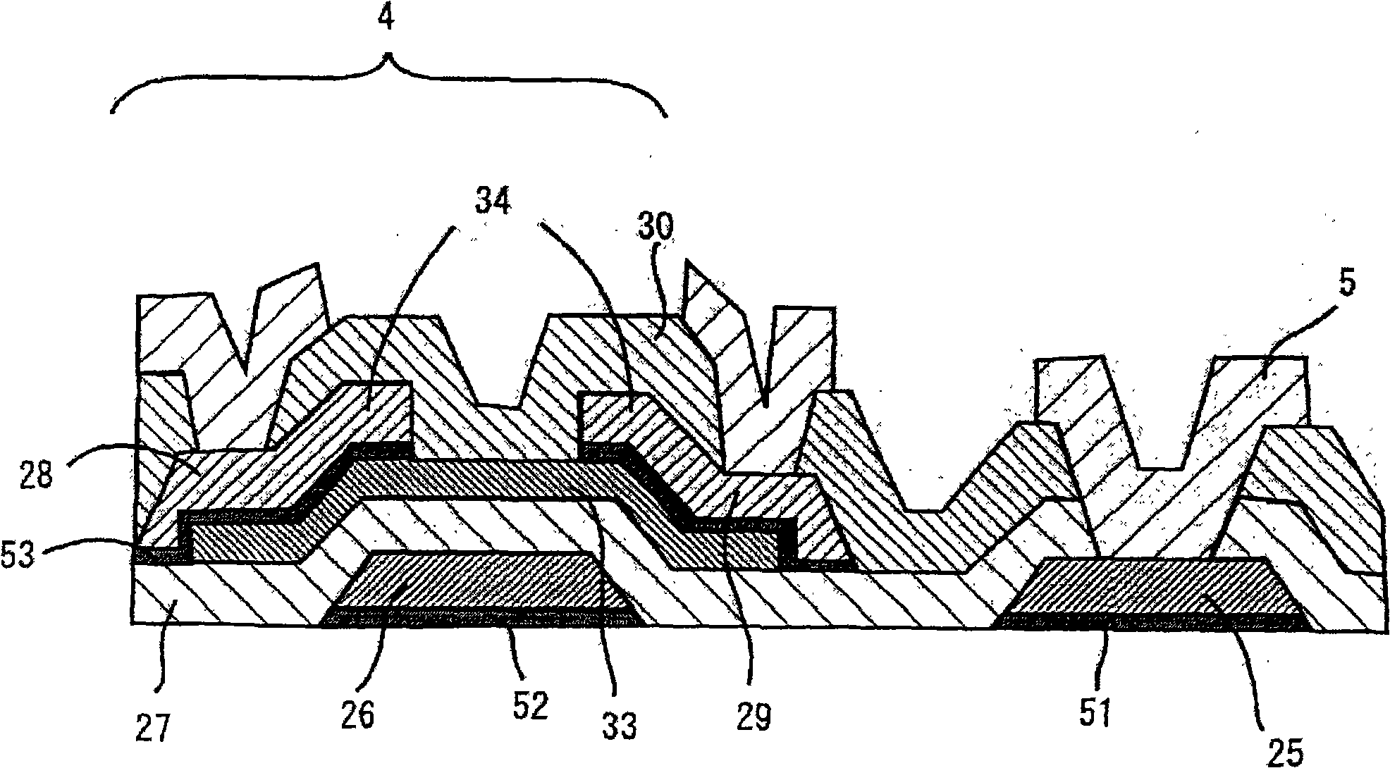
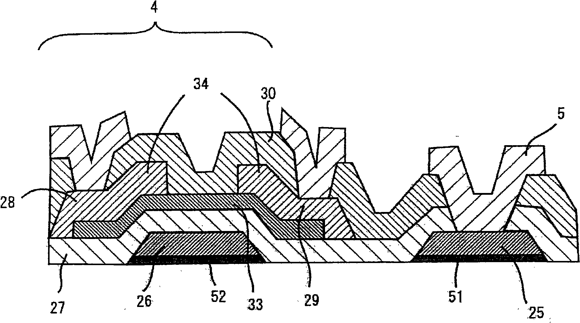
[0143] image 3 It is a schematic cross-sectional view illustrating an embodiment of the amorphous silicon TFT substrate of the present invention. exist image 3 , attached with the aforementioned representation of the existing TFT substrate figure 2 same number. According to the present embodiment, as will be described in detail below, the formation of a layer containing oxygen (oxygen-containing layer) was confirmed.
[0144] exist image 3 Among them, the source-drain wiring 34 electrically connected to the source electrode 28 and the drain electrode 29 is composed of an oxygen-containing layer and a pure Cu or Cu alloy film (such as Cu-0.5 atomic % Mn alloy, Cu-0.34 atomic % Ni alloy , Cu-1.3 atomic % Zn alloy, Cu-1.0 atomic % Mg alloy), and the oxygen-containing layer is formed to cover the amorphous silicon channel layer 33 . The configuration of the source-drain wiring 34 is shown in the later-described Figure 4 (e) and Figure 4 (f).
[0145] If compared fi...
Embodiment 1~2
[0166] (Examples 1-2, Comparative Example 1)
[0167] If a source-drain electrode of a Cu alloy film with an oxygen-containing layer is used, even if the barrier metal layer is omitted, the diffusion of Cu to the half-layer body layer can be suppressed, thereby obtaining good TFT characteristics. In the following embodiment 1 In ~2, various experiments were performed to investigate this point. In Examples 1 and 2, the oxygen-containing layer was formed by the same plasma oxidation method as in Embodiment 1 described above. The specific experimental conditions and evaluation methods are as follows.
[0168] (source-drain electrodes)
[0169] In Example 1, Cu-0.5 atomic % Mn described in Embodiment 1 was used as the wiring material for the source-drain electrodes.
[0170] In Example 2, pure Cu is used to replace Cu-0.5 atomic % Mn in the aforementioned Embodiment 1.
[0171] In Comparative Example 1, although pure Cu was used, oxygen plasma treatment was not performed.
[...
Embodiment 3
[0191] In this example, in addition to performing the plasma oxidation method under various conditions (conditions 1 to 7) shown in Table 1 in the aforementioned example 2 (using pure Cu) to form an oxygen-containing layer, A TFT was produced in the same manner as in Example 1, and various heat treatments similar to those in Example 1 were performed on this TFT. For comparison, a TFT not subjected to heat treatment was also prepared. In either case oxygen was used as the carrier gas.
[0192] Among the plasma oxidation treatment conditions 1 to 7 shown in Table 1, the conditions 1, 2, 4, 5, and 7 are examples set within the range specified by the present invention. In particular, the pressure of the condition 2 is more the same, and the condition 5 The higher power is an example of setting within the preferable range prescribed by the present invention. On the other hand, the condition 3 where the pressure is as low as 38 Pa and the condition 6 as long as 600 seconds are exa...
PUM
| Property | Measurement | Unit |
|---|---|---|
| Thickness | aaaaa | aaaaa |
| Thickness | aaaaa | aaaaa |
Abstract
Description
Claims
Application Information