Laminate structure including oxide semiconductor thin film layer, and thin film transistor

a thin film layer and laminate technology, applied in the direction of transistors, vacuum evaporation coatings, coatings, etc., can solve the problems of increased carrier concentration and decreased mobility, and achieve excellent tft characteristics and decreased mobility

Active Publication Date: 2013-08-29
IDEMITSU KOSAN CO LTD
View PDF17 Cites 18 Cited by
  • Summary
  • Abstract
  • Description
  • Claims
  • Application Information

AI Technical Summary

Benefits of technology

[0131]The oxide layer (oxide thin film) included in the stacked layer structure obtained by the method according to the invention is a thin film formed of indium and oxygen, a thin film formed of indium, oxygen, and gallium, a thin film formed of indium, oxygen, and aluminum, a thin film formed of indium, oxygen, and zinc, or a thin film formed of indium, oxygen, and tin. The oxide layer may include unavoidable impurities as long as the oxide layer mainly include the above elements. Note that it is desirable that the crystal structure substantially have only an indium oxide bixbyite structure.
[0132]Since a thin film having an indium oxide bixbyite structure that is obtained by controlling the Rrms of the oxide thin film (oxide layer) to 1.0 to 5.3 Å, and then annealing (crystallizing) the oxide thin film (oxide layer) has a configuration in which the crystals of the oxide thin film are arranged in a columnar shape from the surface of the substrate to the surface of the thin film, excellent TFT characteristics can be achieved.
[0133]Whether or not the oxide thin film (oxide layer) has an indium oxide bixbyite structure may be determined by X-ray diffraction (XRD) measurement.
[0134]Note that intense X-rays are observed in a specific direction when X-rays are incident on a crystal in which atoms are arranged regularly, so that a diffraction phenomenon occurs. Specifically, when the optical path difference of X-rays scattered at each position is an integral multiple of the wavelength of the X-rays, the amplitude of the waves increases since the phases of the waves coincide, so that the diffraction phenomenon occurs.
[0135]Since a substance forms a crystal having specific regularity, the type of compound can be identified by utilizing X-ray diffraction. It is also possible to evaluate the size of crystals (crystalline order), the distribution state of the orientation of crystals present in the material (crystal orientation), and the residual stress applied to the crystals.
[0136]The density of the oxide layer (oxide thin film) obtained by the method according to the invention is preferably 6.2 g / cm3 or more, and more preferably 6.4 g / cm3 or more. If the density of the oxide layer (oxide thin film) is less than 6.2 g / cm3, the degree of 5 s orbital overlap of In that takes part in carrier conduction may decrease, so that a decrease in mobility may occur.

Problems solved by technology

However, the thin film transistor disclosed in Patent Document 4 that utilizes In2O3 crystals as the channel layer has normally-on properties, and an increase in carrier concentration and a decrease in mobility may occur due to the crystallization step.

Method used


Image

  • Laminate structure including oxide semiconductor thin film layer, and thin film transistor
  • Laminate structure including oxide semiconductor thin film layer, and thin film transistor
  • Laminate structure including oxide semiconductor thin film layer, and thin film transistor

Examples


examples 1 to 13

[1] Fabrication of Hall Effect Measurement Device, XRD Evaluation Device, AFM Evaluation Device, SIM Evaluation Device, and Cross-Sectional TEM Evaluation Device

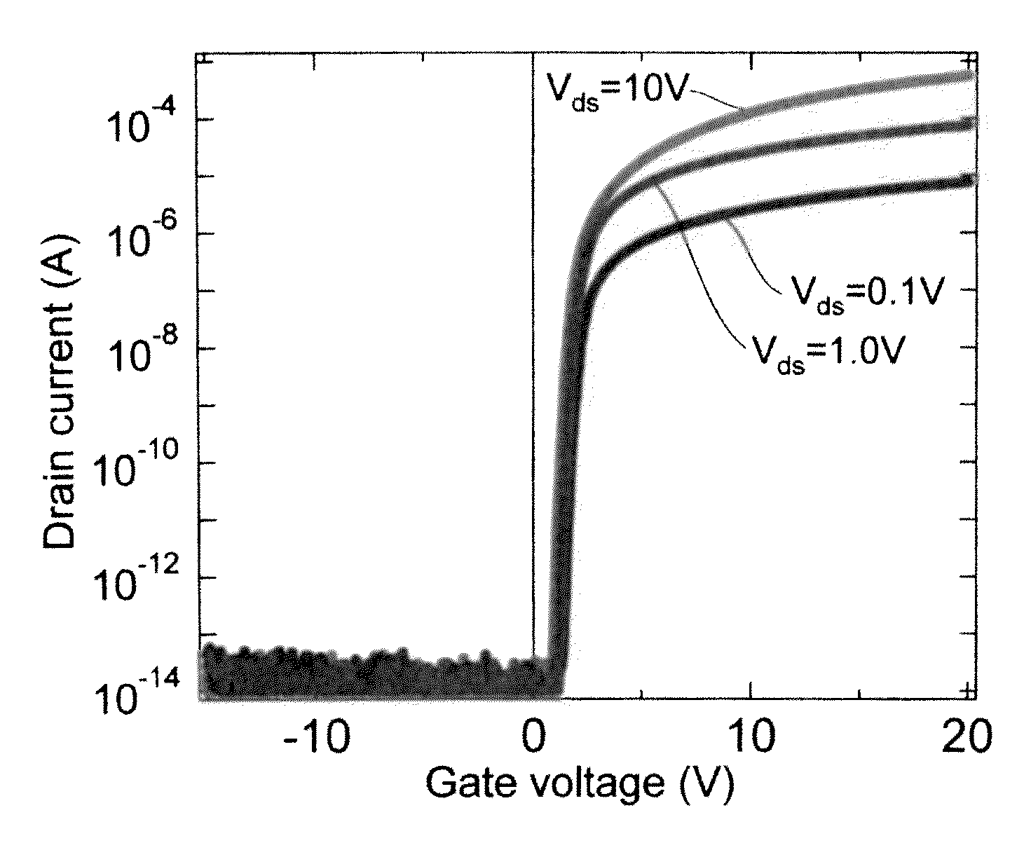
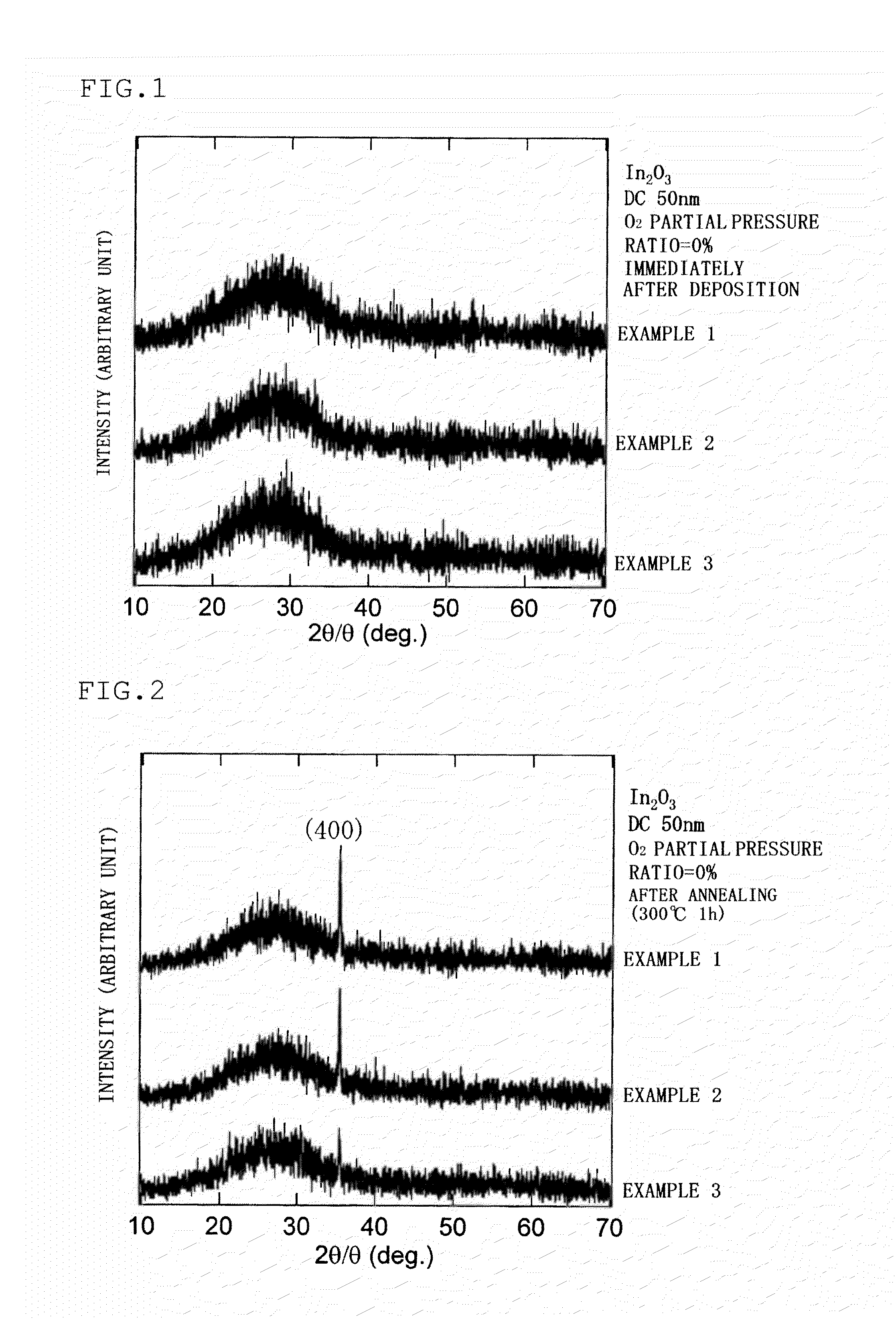
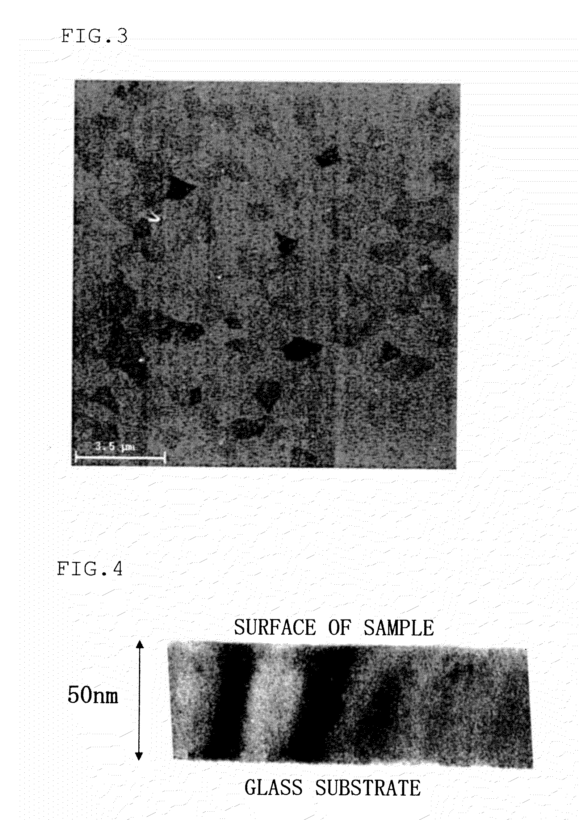
[0162]A 4-inch target formed of an oxide having the composition shown in Table 1, and a slide (“#1737” manufactured by Corning) as a substrate (insulating layer included in stacked layer structure) were placed in a magnetron sputtering system. An amorphous film having a thickness of 50 nm was formed on the slide by DC magnetron sputtering under the following conditions. Ar gas, O2 gas, and H2O gas were introduced when forming the amorphous film in the partial pressure ratio shown in Table 1. The substrate on which the amorphous film was formed was heated at 300° C. for 1 hour in air to crystallize the amorphous film to obtain an oxide semiconductor film (oxide layer included in stacked layer structure).

[0163]It was confirmed by ICP-AES analysis that the atomic ratio of the elements contained in the crystallized oxide thin fi...

example 14

[0199]A thin film transistor and a thin film evaluation device were fabricated, and evaluated in the same manner as in Example 1, except that the amorphous film was formed by AC sputtering under the conditions shown in Table 3 using the system disclosed in JP-A-2005-290550, and annealed. The results are shown in Table 3.

[0200]AC sputtering was performed using the system illustrated in FIG. 8.

[0201]Specifically, six targets 31a to 31f (Zn / (Zn+In)=0.04, width: 200 mm, length: 1700 mm, and thickness: 10 mm) were disposed at an interval of 2 mm in parallel to the widthwise direction of the substrate (not illustrated in FIG. 8). The width of the magnetic field-forming means 40a to 40f was the same as that (200 mm) of the targets 31a to 31f. Ar and H2O (sputtering gas) were introduced into the system from the gas supply system in a flow rate ratio of 99:1. The pressure of the atmosphere was 0.5 Pa. The power supplied from the alternating power source was set to 3 W / cm2 (=10.2 kW / 3400 cm2)...

examples 15 to 18

[0203]A semiconductor thin film was obtained in the same manner as in Example 14, except that the composition of the target and the sputtering conditions were changed as shown in Table 3. A thin film transistor and a thin film evaluation device were fabricated, and evaluated in the same manner as in Example 14. It was found by Hall measurement that a semiconductor was obtained. The results are shown in Table 3.


PUM

PropertyMeasurementUnit
average crystal diameteraaaaaaaaaa
frequencyaaaaaaaaaa
crystal diameteraaaaaaaaaa

Abstract

A stacked layer structure including an oxide layer and an insulating layer, the oxide layer having a carrier concentration of 1018/cm3 or less and an average crystal diameter of 1 μm or more; and the crystals of the oxide layer being arranged in a columnar shape on the surface of the insulating layer.

Description

TECHNICAL FIELD[0001]The invention relates to a stacked layer structure that includes an oxide semiconductor thin film layer, and a thin film transistor that utilizes the oxide semiconductor thin film layer as a channel layer.BACKGROUND ART[0002]A field effect transistor has been widely used as a unit electronic device of a semiconductor memory integrated circuit, a high-frequency signal amplifier device, a liquid crystal drive device, and the like. The field effect transistor is an electronic device that is most widely put to practical use at present.[0003]In recent years, development of displays (display apparatuses) has rapidly progressed, and a thin film transistor (TFT) has been widely used for a display (e.g., liquid crystal display (LCD), electroluminescence (EL) display, or field emission display (FED)) as a switching device for applying a drive voltage to the display element.[0004]A transparent semiconductor thin film formed of a metal oxide (particularly zinc oxide crystal...

Claims


Application Information

Patent Timeline
Patent Type & Authority Applications(United States)
IPC IPC(8): H01L29/786H01L29/66
CPCH01L29/7869H01L21/02488H01L21/02667H01L21/02554C23C14/086H01L21/02631H01L29/66742H01L29/66969H01L21/02565H01L21/324H01L29/04H01L29/06H01L29/78606
Inventor EBATA, KAZUAKITOMAI, SHIGEKAZUTSURUMA, YUKIMATSUZAKI, SHIGEOYANO, KOKI
Owner IDEMITSU KOSAN CO LTD
Why Eureka
Try Eureka