Oxide for semiconductor layer of thin film transistor, sputtering target, and thin-film transistor

A technology of thin film transistors and sputtering targets, which is applied in the manufacture of transistors, semiconductor devices, semiconductor/solid-state devices, etc. It can solve the problems of unstable TFT characteristics, reduced mobility, and increased costs, and achieve switching characteristics and stress resistance. Excellent, small change in threshold voltage, and high reliability

Inactive Publication Date: 2013-08-28
KOBE STEEL LTD
View PDF6 Cites 7 Cited by
  • Summary
  • Abstract
  • Description
  • Claims
  • Application Information

AI Technical Summary

Problems solved by technology

However, even with this method, in order for Al 2 o 3 film formation, the film formation chamber still needs to be re-prepared, and the increase in cost cannot be avoided
[0009] On the other hand, among the metals (In, Ga, Zn) constituting IGZO, Ga is excellent in increasing the band gap and has a strong bond with oxygen, but it has the effect of lowering the mobility.
Therefore, although Ga-free In-Zn-O oxide semiconductor (IZO) can achieve high mobility compared to IGZO, it is prone to oxygen deficiency and has the problem that TFT characteristics tend to become unstable.

Method used


Image

  • Oxide for semiconductor layer of thin film transistor, sputtering target, and thin-film transistor
  • Oxide for semiconductor layer of thin film transistor, sputtering target, and thin-film transistor
  • Oxide for semiconductor layer of thin film transistor, sputtering target, and thin-film transistor

Examples


Embodiment 1

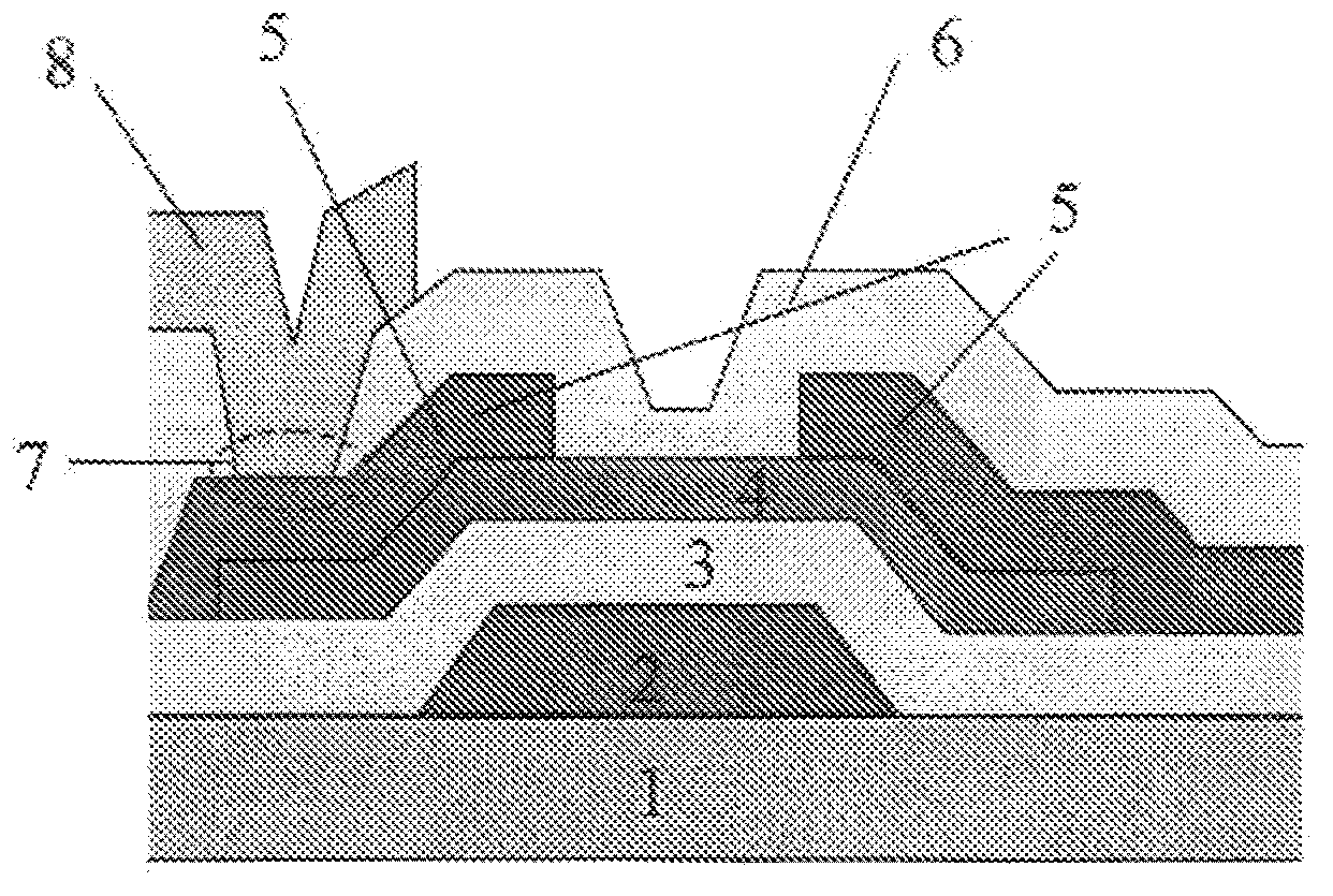
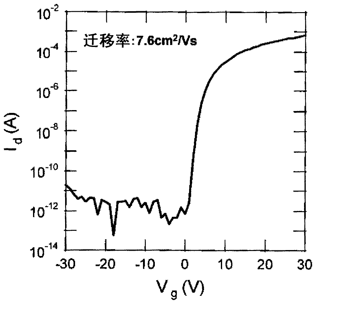
[0083] Based on the above method, the production figure 1 Each characteristic of the thin film transistor (TFT) shown in was evaluated.

[0084] First, on a glass substrate (EAGLE2000 manufactured by Corning, 100mm in diameter x 0.7mm in thickness), a 100nm Mo thin film as a gate electrode, and a gate insulating film of SiO 2 (200nm) film formation. The gate electrode was formed by a DC sputtering method using a pure Mo sputtering target. Set the sputtering conditions as follows: room temperature, film forming power density: 3.8W / cm 2 , Air pressure: 2mTorr, Ar gas flow: 20sccm. In addition, the gate insulating film adopts the plasma CVD method, in the carrier gas: SiH 4 with N 2 Mixed gas of O, film forming power: 1.27W / cm 3 , Film forming temperature: film forming under the condition of 320℃. The air pressure at the time of film formation was set to 133Pa.

[0085] Next, oxide thin films having various compositions described in Table 1 described later were formed int...

Embodiment 2

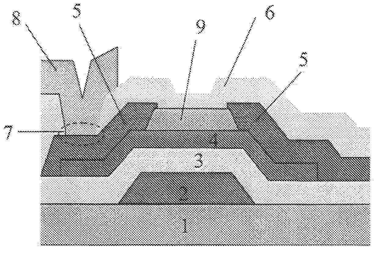
[0142] In this example, the relationship between the density of the oxide semiconductor film and the TFT characteristics was investigated for oxides having the compositions shown in Table 2. Specifically, while measuring the density of the oxide film (thickness: 100 nm) by the following method, TFTs were produced in the same manner as in Example 1 above, and field-effect mobility was measured. In Table 2, the composition (In-Zn-Sn-O) of No. 1 and 2 oxides in Table 2 is the same as No. 2 in Table 1 above; the composition of No. 3 and 4 oxides in Table 2 (In-Zn-Al-O) is the same as No. 4 in the above table 1; the composition of oxides (In-Zn-Ti-O) of No. 5 and 6 in the table 2 is the same as No. 6 in the above table 1 The composition (In-Zn-La-O) of the oxide of No.7 of Table 2 is the same as No.8 of the above-mentioned Table 1; the composition of the oxide of No.8 of Table 2 (In-Zn-Mg-O ) is the same as No. 9 in the above-mentioned Table 1; the composition (In-Zn-Nb-O) of the ...


PUM

PropertyMeasurementUnit
densityaaaaaaaaaa
thicknessaaaaaaaaaa

Abstract

This oxide for a semiconductor layer of a thin film transistor contains: In; Zn; and at least one element (group X element) selected from a group formed from Al, Si, Ta, Ti, La, Mg, and Nb. According to the present invention, the switching characteristics and resistance to stress are excellent in a thin-film transistor provided with an In-Zn-O oxide semiconductor that does not contain Ga, and specifically, an oxide for a semiconductor layer of a thin-film transistor that has a small amount of change in the threshold voltage before and after the application of a positive bias stress and superior stability can be provided.

Description

technical field [0001] The present invention relates to an oxide for a semiconductor layer of a thin film transistor, a sputtering target for forming the oxide, and a thin film transistor including the oxide, wherein the thin film transistor is used for a liquid crystal display, an organic EL Display devices such as monitors. Background technique [0002] Compared with the general-purpose amorphous silicon (a-Si), because the amorphous (amorphous) oxide semiconductor has high carrier mobility (also called field effect mobility. Hereinafter, it is simply called "transfer In the case of "ratio".), the optical bandgap is large, and it can be formed into a film at low temperature, so it is expected to be used in next-generation displays that require large, high-resolution, and high-speed drives, and resin substrates with low heat resistance. [0003] Because among oxide semiconductors, especially amorphous oxide semiconductors (In-Ga-Zn-O, hereinafter referred to as "IGZO") con...

Claims


Application Information

Patent Timeline
Patent Type & Authority Applications(China)
IPC IPC(8): H01L29/786H01L21/336H01L21/363
CPCC23C14/086C23C14/3414H01L21/02554H01L21/02565H01L21/02631H01L29/7869H01L27/016H01L27/1225H10K59/1213
Inventor 森田晋也三木绫安野聪钉宫敏洋岸智弥
Owner KOBE STEEL LTD
Why Eureka
Try Eureka