Gallium nitride compound semiconductor light-emitting device and method for manufacturing same

A light-emitting element and manufacturing method technology, applied to semiconductor devices, electrical components, circuits, etc., can solve the problems of increased number of processes, increased manufacturing costs, and damage to the surface of gallium nitride-based compound semiconductors, etc., to reduce contact resistance, The effect of high light extraction efficiency

Active Publication Date: 2008-12-24
TOYODA GOSEI CO LTD
View PDF3 Cites 6 Cited by
  • Summary
  • Abstract
  • Description
  • Claims
  • Application Information

AI Technical Summary

Problems solved by technology

[0013] However, in the gallium nitride-based compound semiconductor light-emitting device described in Patent Document 3, heat treatment must be performed after the metal layer including the Mg layer and the Au layer is provided, and the process of removing the metal layer must be performed. The problem that the number of processes is greatly increased and the manufacturing cost is increased
In addition, when removing the aforementioned Au layer, it is necessary to use a strong acid such as aqua regia, which may damage the surface of the gallium nitride-based compound semiconductor.

Method used


Image

  • Gallium nitride compound semiconductor light-emitting device and method for manufacturing same
  • Gallium nitride compound semiconductor light-emitting device and method for manufacturing same
  • Gallium nitride compound semiconductor light-emitting device and method for manufacturing same

Examples


no. 1 approach

[0101] Hereinafter, regarding the first embodiment of the gallium nitride-based compound semiconductor light-emitting device of the present invention, reference will be made as appropriate. Figure 1~4 while explaining.

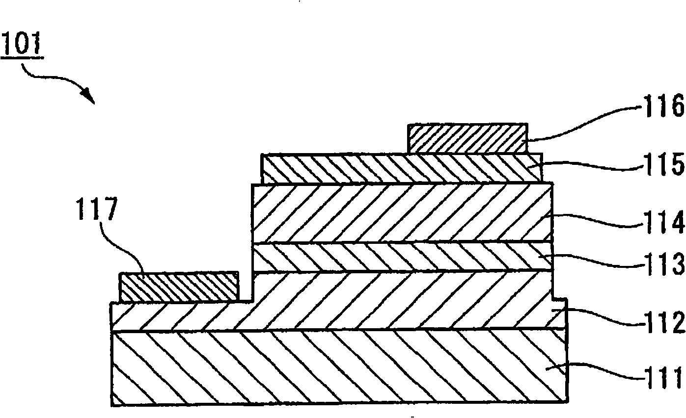
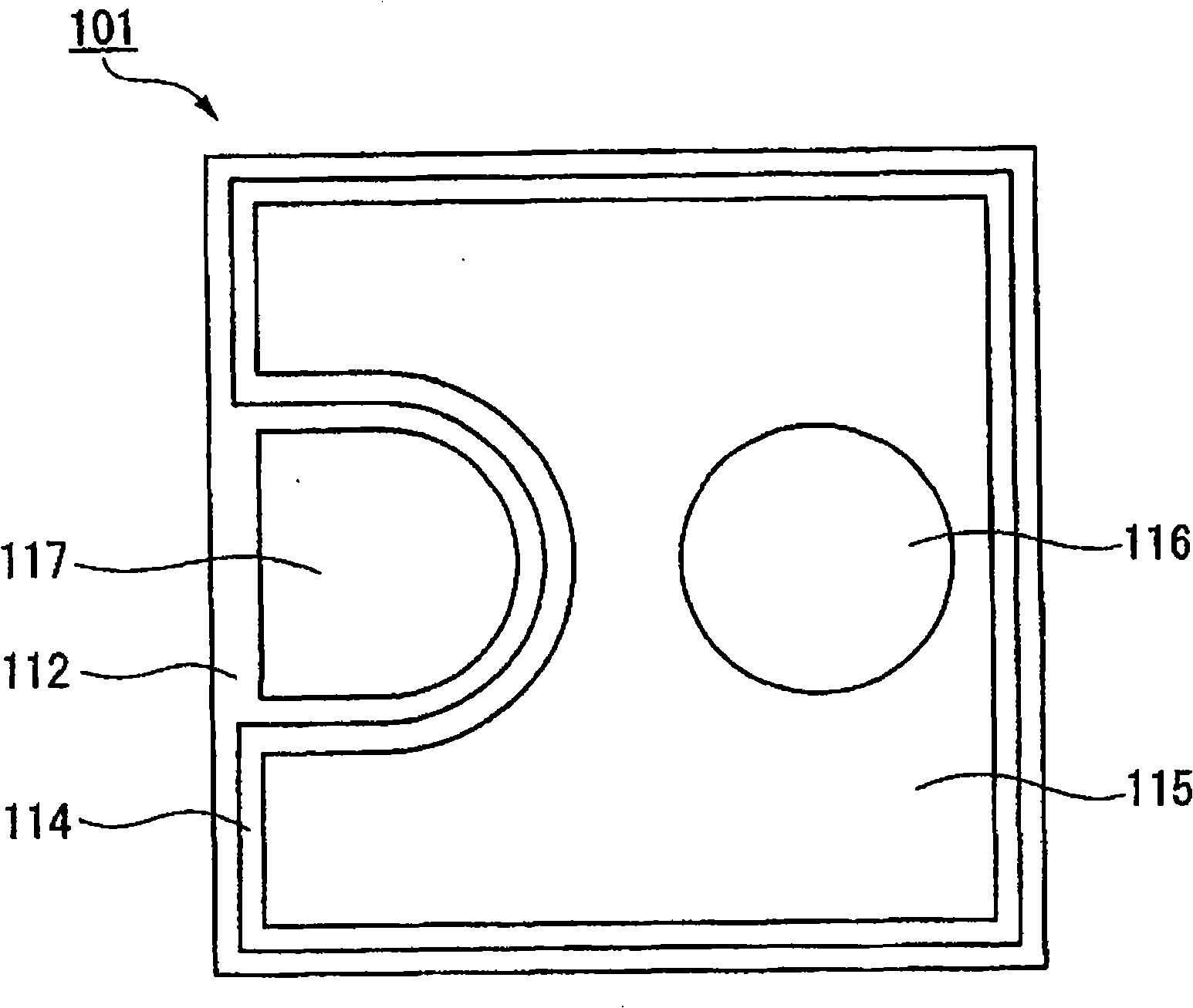
[0102] shown in figure 1 The gallium nitride-based compound semiconductor light-emitting element 101 of this embodiment is schematically configured such that an n-type GaN layer 112 , a light-emitting layer 113 , and a p-type GaN layer (p-type semiconductor layer) 114 are formed on a substrate 111 in this order. On the aforementioned p-type GaN layer 114 of the stacked gallium nitride-based compound semiconductor element, a positive electrode 115 formed of a light-transmitting conductive oxide film containing a dopant is stacked, and the p-type GaN layer 114 and the positive electrode (light-transmitting The dopant concentration at the interface of the conductive oxide film 115 is higher than that of the bulk of the translucent conductive oxide film forming ...

experiment example 1

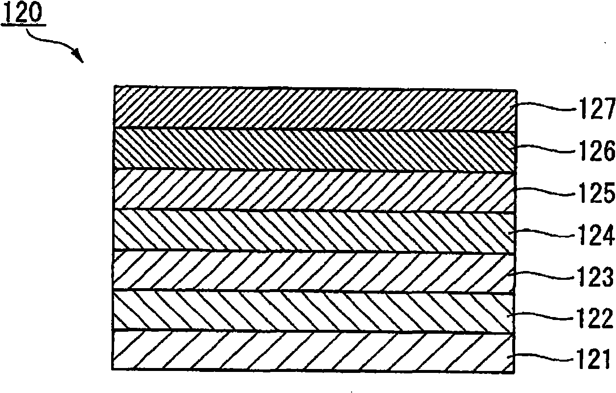
[0144] image 3 , shows a schematic cross-sectional view of an epitaxial structure produced for use in the gallium nitride-based compound semiconductor light-emitting device of this example. and, in figure 1 and figure 2 , shows a schematic cross-sectional view and a schematic plan view of the gallium nitride-based compound semiconductor light-emitting device of the present invention, and will be described below with appropriate reference.

[0145] (Manufacturing of GaN-based compound semiconductor light-emitting devices)

[0146] The multilayer structure of the gallium nitride-based compound semiconductor light-emitting element 120 is composed of a substrate 121 including a c-plane ((0001) crystal plane) of sapphire, with a buffer layer (not shown) including AlN interposed therebetween. Doped GaN base layer (layer thickness=2 μm) 122, Si-doped n-type GaN contact layer (layer thickness=2 μm, carrier concentration=1×10 19 cm -3 ) 123, Si-doped n-type Al 0.07 Ga 0.93 N c...

experiment example 2-5

[0157] Before the formation of the translucent conductive oxide film layer containing ITO, a translucent conductive oxide film contact layer of about 2 nm was formed, and a gallium nitride-based compound semiconductor light-emitting device was produced in the same manner as in Experimental Example 1.


PUM

PropertyMeasurementUnit
thicknessaaaaaaaaaa
thicknessaaaaaaaaaa
thicknessaaaaaaaaaa

Abstract

Disclosed is a gallium nitride compound semiconductor light-emitting device having high light extraction efficiency and low driving voltage (Vf). Specifically disclosed is a gallium nitride compound semiconductor light-emitting device wherein a light-transmitting conductive oxide film containing a dopant is arranged on a p-type semiconductor layer. In this gallium nitride compound semiconductor light-emitting device, the dopant concentration at the interface between the p-type semiconductor layer and the light-transmitting conductive oxide film is set higher than the bulk dopant concentration of the light-transmitting conductive oxide film, thereby reducing the contact resistance between the p-type semiconductor layer and the light-transmitting conductive oxide film.

Description

technical field [0001] The present invention relates to a gallium nitride-based compound semiconductor light-emitting element, in particular to a gallium nitride-based compound semiconductor light-emitting element with a low driving voltage (Vf) and a manufacturing method thereof. [0002] This application claims priority based on Japanese Patent Application No. 2005-360288 filed on December 14, 2005 and Japanese Patent Application No. 2005-360289 filed on December 14, 2005 in Japan, and is incorporated herein by reference. their content. Background technique [0003] In recent years, gallium nitride-based compound semiconductor light-emitting elements have attracted attention as short-wavelength light-emitting elements. This gallium nitride-based compound semiconductor light-emitting device uses sapphire single crystal as a substrate, various oxides and III-V compounds as substrates, and on this substrate, metal organic vapor phase chemical reaction method (MOCVD method) o...

Claims


Application Information

Patent Timeline
Patent Type & Authority Applications(China)
IPC IPC(8): H01L33/00H01L33/32H01L33/38H01L33/42
Inventor 福永修大篠原裕直大泽弘
Owner TOYODA GOSEI CO LTD
Why Eureka
Try Eureka