Adhesive for LED chip

A technology of LED chips and bonding glue, which is applied in the direction of adhesives, inorganic adhesives, electrical components, etc., can solve the problems of adding LED chips, low thermal conductivity, unfavorable heat dissipation of devices and high temperature working stability, etc., to achieve increased bonding The effect of strength, high brightness, and good chemical stability

Inactive Publication Date: 2008-12-31
包书林 +1
View PDF0 Cites 4 Cited by
  • Summary
  • Abstract
  • Description
  • Claims
  • Application Information

AI Technical Summary

Problems solved by technology

[0003] The chip bonding material commonly used in the LED industry is epoxy resin (EPOXY), but EPOXY has a high thermal resistance of 250-300°C / W and a low thermal conductivity (1-2W / m.K). The structure is epoxy resin + silver powder filled thermal and conductive structure, such a structure TG (TG point refers to the glass transition temperature, generally when the working temperature exceeds this temperature for a long time, the various functions of the polymer will change and fail) The low point is extremely unfavorable to the heat dissipation of the device and the stability of high-temperature work. According to statistical analysis, the attenuation and failure of the current LED light intensity are mostly caused by the instability of the bonding material when the chip is working at high temperature. With the increase of LED power It is necessary to strengthen the thermal control of the chip and increase the thermal conductivity of the LED chip

Method used


Image

  • Adhesive for LED chip
  • Adhesive for LED chip
  • Adhesive for LED chip

Examples


Embodiment 1

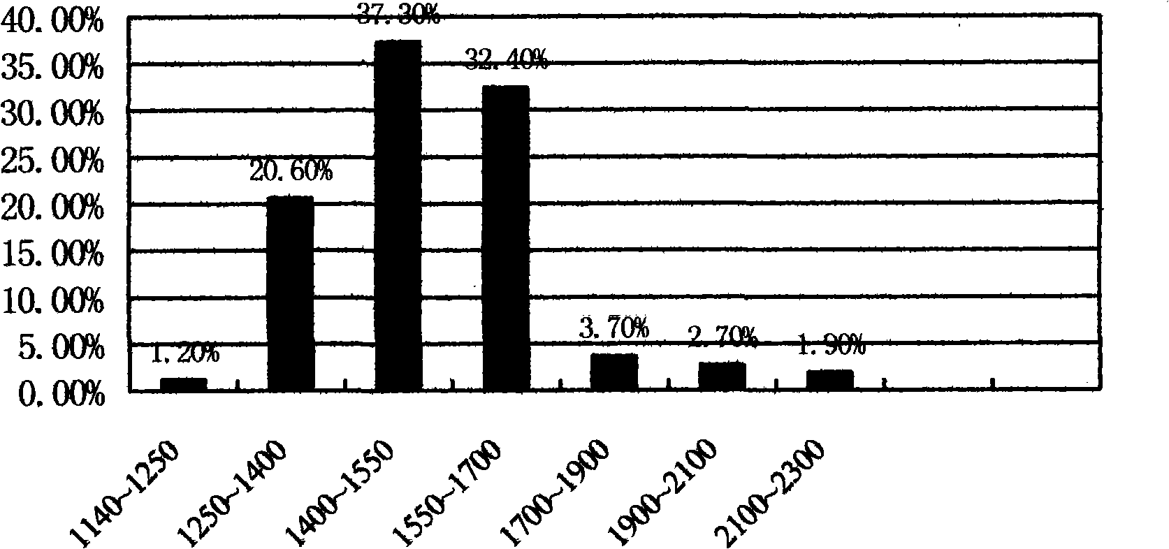
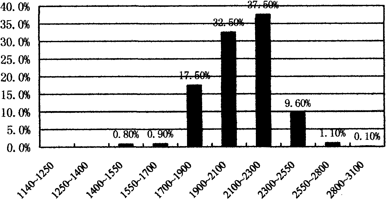
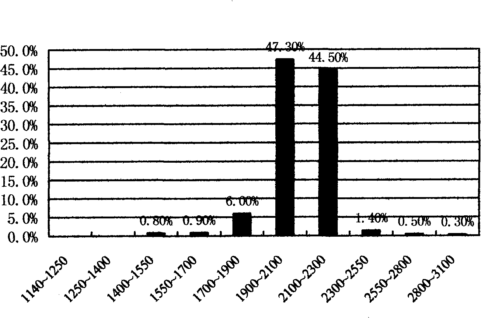
[0015] Using different characteristics of chip bonding glue, using the same LED chip, the same packaging process and packaging glue to make white PLCC LED, the test distribution results of the luminous intensity are as follows Figure 1~3 As shown (the test instrument is WEIMING LED-638T, test conditions: Ta: 25°C, RH 45% IF = 20mA)

[0016] The test results show that, using the same LED chip, the same packaging process, and using adhesives with different characteristics, under the premise that the electrical properties and CIE blocks of white PLCC LEDs are basically the same, the brightness will be very different. This is due to the different characteristics The different adhesives are caused by the difference in light transmittance, refractive index, etc. It can be seen from the comparison that the material of the present invention will be of great help to improve the brightness of the LED.

Embodiment 2

[0018] Compare the brightness decay curves of epoxy resin and silicone bonding materials, such as Figure 4 , Figure 5 As shown, test conditions: Ta: 25°C, RH 45, IF=20mA, 1000HRS. Through the verification of the overall reliability experiment, the reliability of the bonding material of the present invention is better than that of the EPOXY structure.

Embodiment 3

[0020] A kind of LED chip bonding glue, the composition of this chip bonding glue is: the transparent optical silica gel (Dow Corning OE-6660 Part A / B TransparentSilicone Resin (Dow Corning Corporation OE-6660A / B component, transparent silicone resin)), also contains AL which accounts for 10-20% of the weight of silica gel 2 o 3 With silica gel weight 2 ~ 10% SiO 2 Powder and sedimentation inhibitor. Precipitation inhibitor is cyclohexanone or ethyl acetate; AL 2 o 3 and SiO 2 Particle size 50m 2 / g.


PUM


Abstract

Disclosed is an LED chip bonding adhesive, containing transparent optical silica gel at hardness higher or equal to 35Shore D and viscosity coefficient higher or equal to 1.5, AL2O3 which is 10-20% of the weight of the silica gel, and powder and sedimentation retardant which are 2-10%of the weight of the silica gel. By adding nano inorganic particle powder into SILICONE, thermal conductivity and bonding strength of the silicone resin are increased, making the silicone resin have enough bonding strength and thermal conductivity after being solidified; meanwhile, the optical transmission of the LED chip is greatly improved; the LED chip bonding adhesive can make the LED higher in brightness and lower in cost; therefore, the LED chip bonding adhesive is the best substitute material for bonding the chip of a double-electrode LED.

Description

1. Technical field [0001] The invention belongs to an LED packaging material, in particular to a double-electrode white light LED for illumination, a chip fixing bonding material for effectively improving its brightness and increasing the working stability of the LED. 2. Background technology [0002] Existing technology: LED is a light-emitting element composed of semiconductor materials, which uses the combination of electrons and holes in the semiconductor to emit photons and generate different frequency spectra. Because of its small size, long life, high photoelectric conversion efficiency, and fast response speed , energy saving, and environmental protection, so it can become the core of the future semiconductor lighting source. [0003] The chip bonding material commonly used in the LED industry is epoxy resin (EPOXY), but EPOXY has a high thermal resistance of 250-300°C / W and a low thermal conductivity (1-2W / m.K). The structure is epoxy resin + silver powder filled t...

Claims


Application Information

Patent Timeline
Patent Type & Authority Applications(China)
IPC IPC(8): C09J1/00H01L33/00H01L33/56
Inventor 包书林孟杰
Owner 包书林
Why Eureka
Try Eureka