LCD and making method thereof

A technology of liquid crystal display and thin film transistor, which is applied in the direction of optics, instruments, electrical components, etc., can solve the problems of reducing the aperture ratio of the display unit, and achieve the effect of reducing the number of cross points, reducing the distance, and increasing the aperture ratio

Inactive Publication Date: 2008-12-31
SHANGHAI SVA LIQUID CRYSTAL DISPLAY
View PDF0 Cites 53 Cited by
  • Summary
  • Abstract
  • Description
  • Claims
  • Application Information

AI Technical Summary

Problems solved by technology

Due to the two layers of insulating film, in order to obtain a larger storage capacitance value, the usual practice is to increase the area of ​​the common electrode line, but this will reduce the aperture ratio of the display unit

Method used


Image

  • LCD and making method thereof
  • LCD and making method thereof
  • LCD and making method thereof

Examples


Embodiment 1

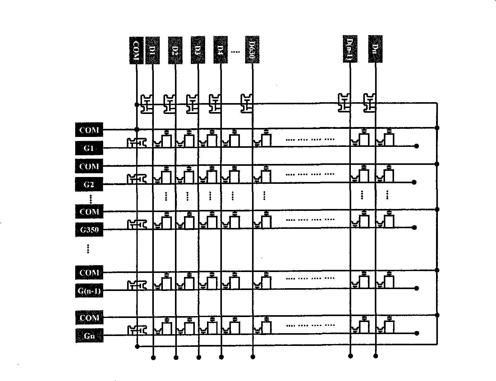
[0043] Figure 4 A schematic diagram of the structure of the array substrate of the present invention is given. Such as Figure 4 As shown, there are two kinds of metal layers on the array substrate of the TFT LCD. The first metal layer forms a group of gate scanning lines, and the second metal layer forms a group of data lines and common electrode lines arranged parallel to each other and perpendicular to the gate scanning lines. Connected scan lines and data lines define display elements within the display area. The potential of the gate scanning line is introduced by the terminal part (formed by the first metal layer) on the left side of the array substrate, the potential of the data line is introduced by the terminal part (formed by the second metal layer) on the upper side of the array substrate, and the common electrode line Potentials are simultaneously introduced from the upper and lower sides of the array substrate. On the upper side of the array substrate, the co...

Embodiment 2

[0057] In addition to the above-mentioned array substrate structure, the following different structural designs can also be implemented on the basis of the above structure according to actual needs.

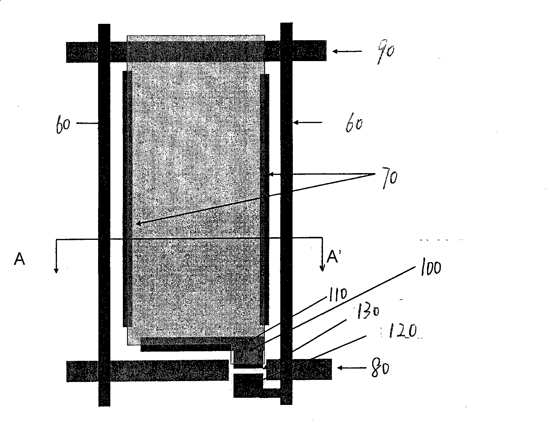
[0058] Such as Figure 6 As shown, the common electrode potential is guided to the opposite side of the data line terminal from the data line terminal module through the first layer of metal. Then lead the potential of the common electrode on the first layer of metal to the common electrode line formed by the second layer of metal in the display area through the contact hole. The contact hole is composed of a via hole on the first metal layer, a via hole on the second metal layer, and a transparent conductive layer respectively covering the two via holes.

Embodiment 3

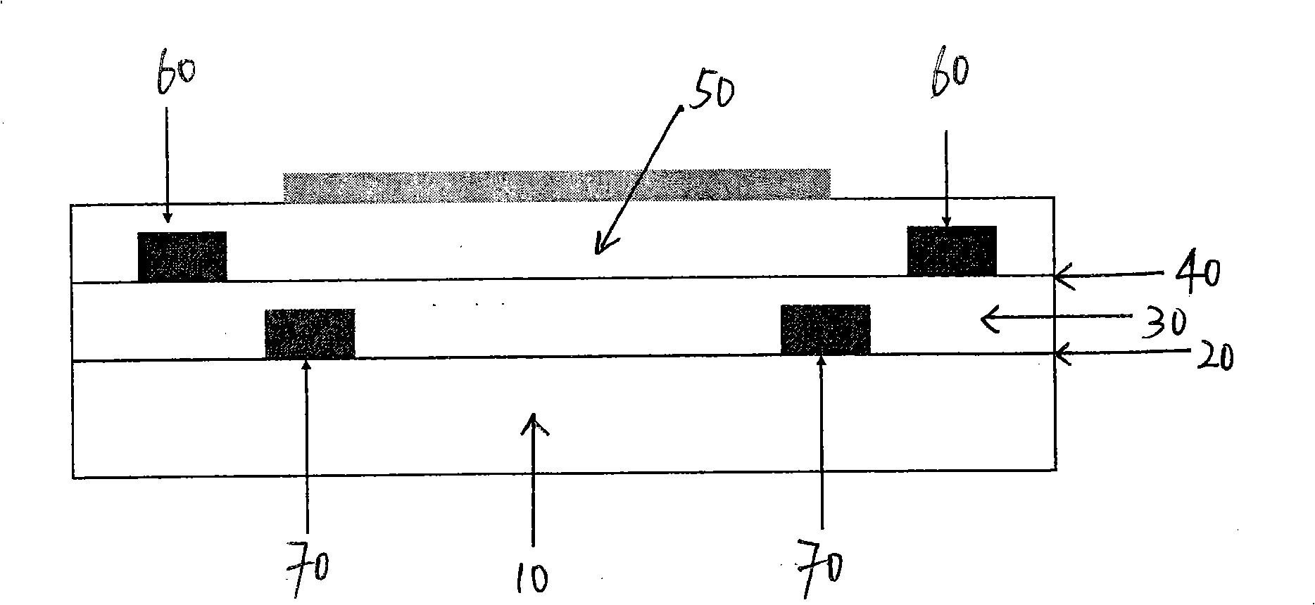
[0060] Such as Figure 7 As shown, the common electrode lines 9 parallel to the data lines can be placed in the center of the display unit in addition to being placed on one side of the display unit. This design can reduce the interference between the data line and the common electrode line, and reduce the probability of short circuit on the same layer that may be caused between the data line and the common electrode line.


PUM


Abstract

The invention provides a liquid crystal display array substrate structure of a film transistor, comprising a substrate and a first metal layer which comprises a gate electrode scanning line, and a gate electrode which are formed on the substrate; a gate electrode insulation layer that is formed on the gate electrode scanning line and the gate electrode; an active layer which is formed on the gate electrode insulation layer; a second metal layer which comprises a data line, a source electrode, a drain electrode and a public electrode line which are formed on the gate insulation layer, wherein, the source electrode and the drain electrode are partly carried on the active layer; a passivation layer which is formed on the data line, the source electrode, the drain electrode and the public electrode line and is formed into a contact hole on the drain electrode; a pixel electrode which is formed on the passivation layer and is connected with the drain electrode by the contact hole on the drain electrode. The invention also provides a preparation method used for a TFT LCD array substrate structure, which improves a state that the public electrode line is originally parallel to the gate electrode scanning line to be a state that the public electrode line is parallel to the data line, reduces the length of each public electrode line in the display area, and reduces the resistance of each public electrode line.

Description

technical field [0001] The invention relates to the field of thin film transistor liquid crystal display (TFT LCD), in particular to a thin film transistor liquid crystal display (TFT LCD) array substrate structure and a manufacturing method thereof. Background technique [0002] A thin film transistor liquid crystal display (TFT LCD) is jointly formed by an array substrate, a color filter substrate, and liquid crystals filled between the two substrates. [0003] figure 1 It is a schematic circuit diagram of a thin film transistor liquid crystal display array substrate circuit in the prior art. As shown in the figure, the gate scanning lines and the common electrode lines are arranged parallel to each other, and cross the data lines and cross the data lines at the same time. In this structure, the common electrode potential is simultaneously introduced to the common electrode lines in the display area on the side of the scanning line terminal and on the side opposite to th...

Claims


Application Information

Patent Timeline
Patent Type & Authority Applications(China)
IPC IPC(8): G02F1/1362H01L27/12
Inventor 马群刚
Owner SHANGHAI SVA LIQUID CRYSTAL DISPLAY
Why Eureka
Try Eureka