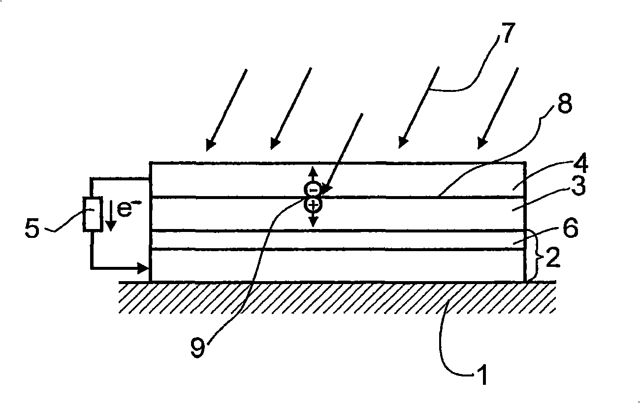
Photovoltaically active semiconductor material and photovoltaic cell
A semiconductor and photovoltaic technology, applied in semiconductor devices, photovoltaic power generation, polycrystalline material growth, etc., can solve problems such as difficult to achieve, incomplete description, etc., to achieve high efficiency
- Summary
- Abstract
- Description
- Claims
- Application Information
AI Technical Summary
Problems solved by technology
Method used
Image
Examples
example
[0079] Execute these examples where the components are Zn 0.99 co 0.01 Te.
[0080] To this end, each element with a purity exceeding 99.99% was weighed into a fused silica tube, residual moisture was removed by heating under reduced pressure, and the tube was flame sealed under reduced pressure.
[0081] In an inclined tube furnace, the tube was heated from room temperature to 1200°C over a period of 60 hours and held at a temperature of 1200°C for 10 hours. The furnace was then turned off and allowed to cool.
[0082] After cooling, the quartz tube was opened under argon and the resulting telluride was ground in an agate mortar to pieces of approximately 1 mm to 5 mm.
[0083] Finally, the ground material is put into a grinding jar of a planetary ball mill. The powder body was infused through n-octane, followed by the addition of grinding balls of 20 mm diameter stabilized zirconia. The volume portion of the grinding balls was about 60%. The grinding jar was closed und...
PUM
 Abstract
Description
Claims
Application Information
