Stackable semiconductor encapsulation construct for multi-cylinder body

A semiconductor and structural technology, which is applied in the framework of high-density package stacking modules and the field of stackable semiconductor package structure, can solve the problems of reducing crack growth and complicating the shape of welding interface, so as to reduce crack growth and increase the reliability of solder joints , The effect of high welding reliability

Inactive Publication Date: 2009-01-28
POWERTECH TECHNOLOGY
View PDF2 Cites 12 Cited by
  • Summary
  • Abstract
  • Description
  • Claims
  • Application Information

AI Technical Summary

Problems solved by technology

[0013] Another object of the present invention is to provide a novel multi-column stackable semiconductor package structure. The technical problem to be solved is to complicate the shape of the soldering interface of the bump group and reduce the possibility of crack growth. making it more practical

Method used


Image

  • Stackable semiconductor encapsulation construct for multi-cylinder body
  • Stackable semiconductor encapsulation construct for multi-cylinder body
  • Stackable semiconductor encapsulation construct for multi-cylinder body

Examples


no. 1 Embodiment

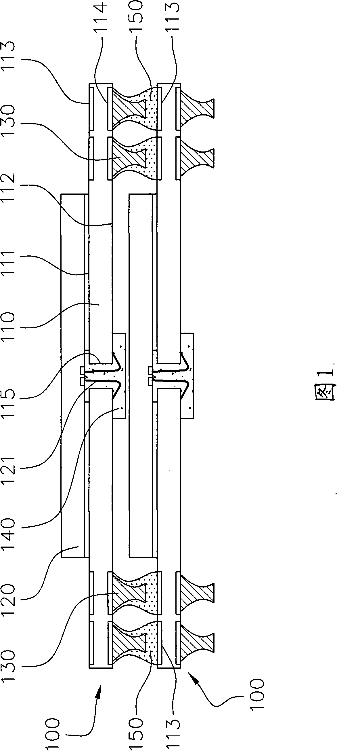
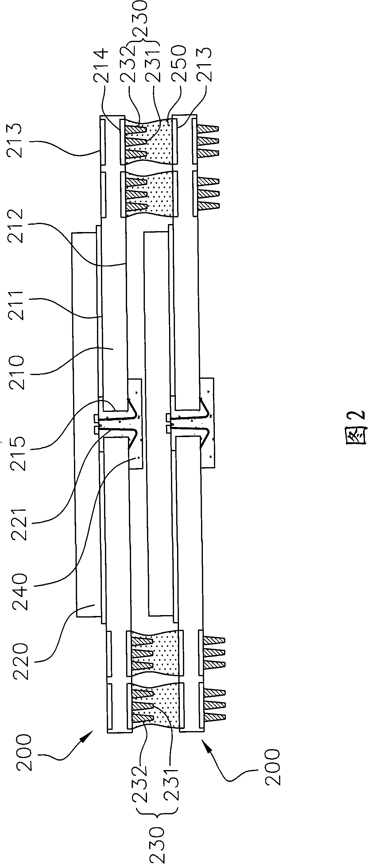
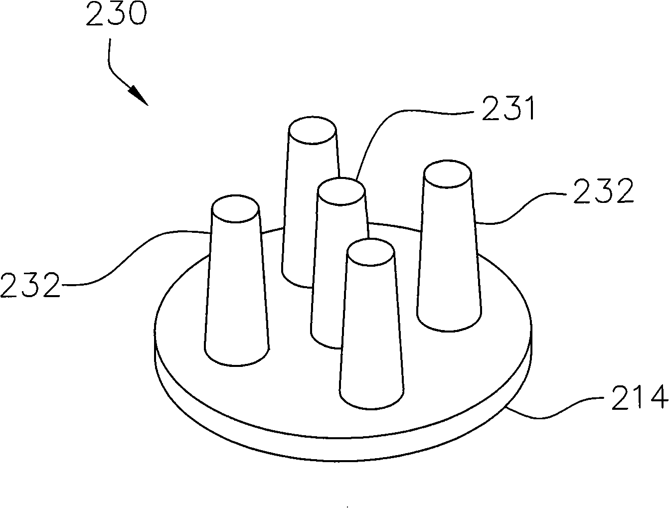
[0080] According to the first specific embodiment of the present invention, a multi-pillar stackable semiconductor package structure is disclosed. Please refer to FIG. 2, which is a schematic cross-sectional view of a stackable semiconductor package structure with multiple pillars stacked on each other according to the first embodiment of the present invention, which is a stack combination of two stackable semiconductor package structures 200, but Without limitation, more stackable semiconductor packaging structures 200 may be stacked on top, for example, three, four or more. Each stackable semiconductor package structure 200 mainly includes a chip carrier 210, a chip 220, and a plurality of lower bump groups 230.

[0081] The chip carrier 210 may be a multilayer printed circuit board with a structure with electrical conduction on both sides. The chip carrier 210 has an upper surface 211 and a lower surface 212, wherein the upper surface 211 is provided with a plurality of transfe...


PUM


Abstract

The invention relates to a polycylinder stackable semiconductor packaging structure. The structure mainly comprises a wafer carrier, a wafer and a plurality of downwards convex block groups, wherein the wafer carrier has a plurality of switchover pads on an upper surface and a plurality of external pads on a lower surface; the wafer is arranged on and is electrically connected with the wafer carrier; the downwards convex block groups are correspondingly arranged on the external pads, and each downwards convex block group connected with each external pad consists of a plurality of conducting cylinders; and a solder filling gap is arranged between adjacent conducting cylinders of the same downwards convex block group. The stackable semiconductor packaging structure is used to increase welding area and perplex the shape of a welding interface, thereby achieving high durability of welding spots and reducing the growing possibility of cracks. In addition, the convex block group arranged on each external pad has the solder filling gap, solder can be filled and stored in the convex block group, so that a plaque does not extrude the solder to cause bridging short circuit even when inclined or warped; therefore, the structure is particularly suitable for practical use.

Description

Technical field [0001] The present invention relates to a three-dimensional stacking technology of semiconductor packaging structures, in particular to a multi-pillar stackable semiconductor packaging structure, which can be applied to a high-density package-on-package module (Package-On-Package module, POP) structure. Background technique [0002] With the development trend of miniaturization of electronic products, the area on the surface of the printed circuit board that can be provided with semiconductor packaging structures is getting smaller and smaller. Therefore, there is a three-dimensional stacking technology of semiconductor packaging structures. A plurality of stackable semiconductor packaging structures are stacked on each other to form a package-on-package module (POP) to meet the small surface bonding area and high density. Requirements for component settings. However, soldering defects are a major problem in the bonding process of the package stack. The soldering ...

Claims


Application Information

Patent Timeline
Patent Type & Authority Applications(China)
IPC IPC(8): H01L23/488H01L23/498
CPCH01L2224/73253H01L2924/15311H01L2924/15331H01L2224/4824H01L2224/16225H01L2924/15321H01L2924/3511H01L2224/73215H01L2224/32225
Inventor 范文正
Owner POWERTECH TECHNOLOGY
Why Eureka
Try Eureka