Thin-film transistor array substrate and preparation method thereof

A technology of thin film transistors and array substrates, applied in the field of thin film transistor array substrates and its production, can solve the problems of increased process time, unfavorable increase in production capacity, and increased total number of times, and achieve high carrier mobility and good component characteristics. Effect

Active Publication Date: 2009-01-28
AU OPTRONICS CORP
View PDF0 Cites 10 Cited by
  • Summary
  • Abstract
  • Description
  • Claims
  • Application Information

AI Technical Summary

Problems solved by technology

[0006] However, in the above-mentioned TDX laser crystallization technology, since the laser beam is irradiated on the amorphous silicon layer on the substrate, and the substrate is moved for scanning operation in the TDX laser crystallization method, the substrate can only be moved no more than two times each time the substrate is moved. 1 / 1 of the laser irradiated area of ​​the substrate
Therefore, when scanning in one direction by the TDX laser crystallization method, not only more laser shots are required, but also the total number of times to move the substrate is increased. In this way, although high-quality polysilicon can be obtained Membrane, but due to the increase of process time, it is not conducive to the improvement of production capacity
In addition, a single scanning pitch is used on the moving substrate or mask. Although the polysilicon in different regions on the substrate is the same, more laser shots are required, and the total number of times to move the substrate or mask is also less. In this way, although the polysilicon film with uniform quality can be obtained, that is, the main grain boundaries of polysilicon at all positions on the substrate are uniformly distributed, but the increase in process time on the substrate is not conducive to the improvement of production capacity.

Method used


Image

  • Thin-film transistor array substrate and preparation method thereof
  • Thin-film transistor array substrate and preparation method thereof
  • Thin-film transistor array substrate and preparation method thereof

Examples


no. 1 example

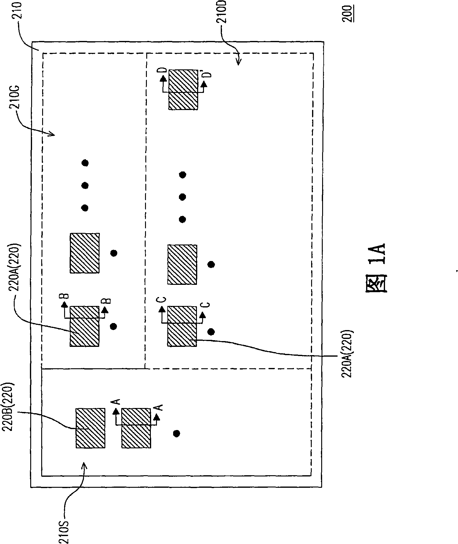
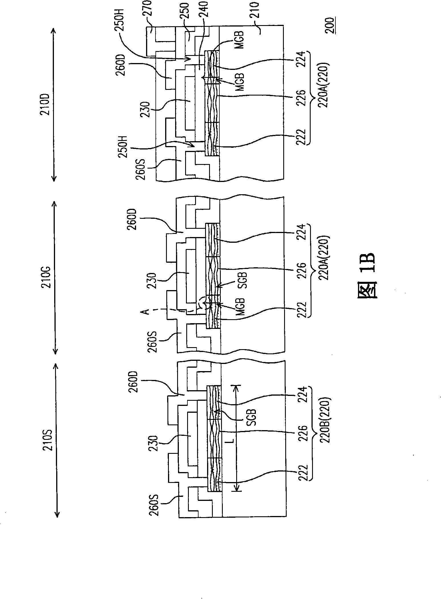
[0060] FIG. 1A is a schematic diagram of a thin film transistor array substrate according to an embodiment of the present invention, and FIG. 1B is a schematic cross-sectional view along line AA, BB and CC in FIG. 1A . Please refer to FIG. 1A and FIG. 1B at the same time. The thin film transistor array substrate 200 includes a substrate 210, a plurality of polysilicon islands 220 disposed on the substrate 210, and a plurality of gates 230. The substrate 210 is mainly divided into a display area 210D, a gate The driving region 210G and the source driving region 210S, and the polysilicon island 220 includes a plurality of first polysilicon islands 220A and a plurality of second polysilicon islands 220B, and the first polysilicon islands 220A are arranged in the display region 210D and the gate in the driving region 210G, and the second polysilicon island 220B is disposed in the source driving region 210S.

[0061] Please continue to refer to FIG. 1B, each polysilicon island 220A...

no. 2 example

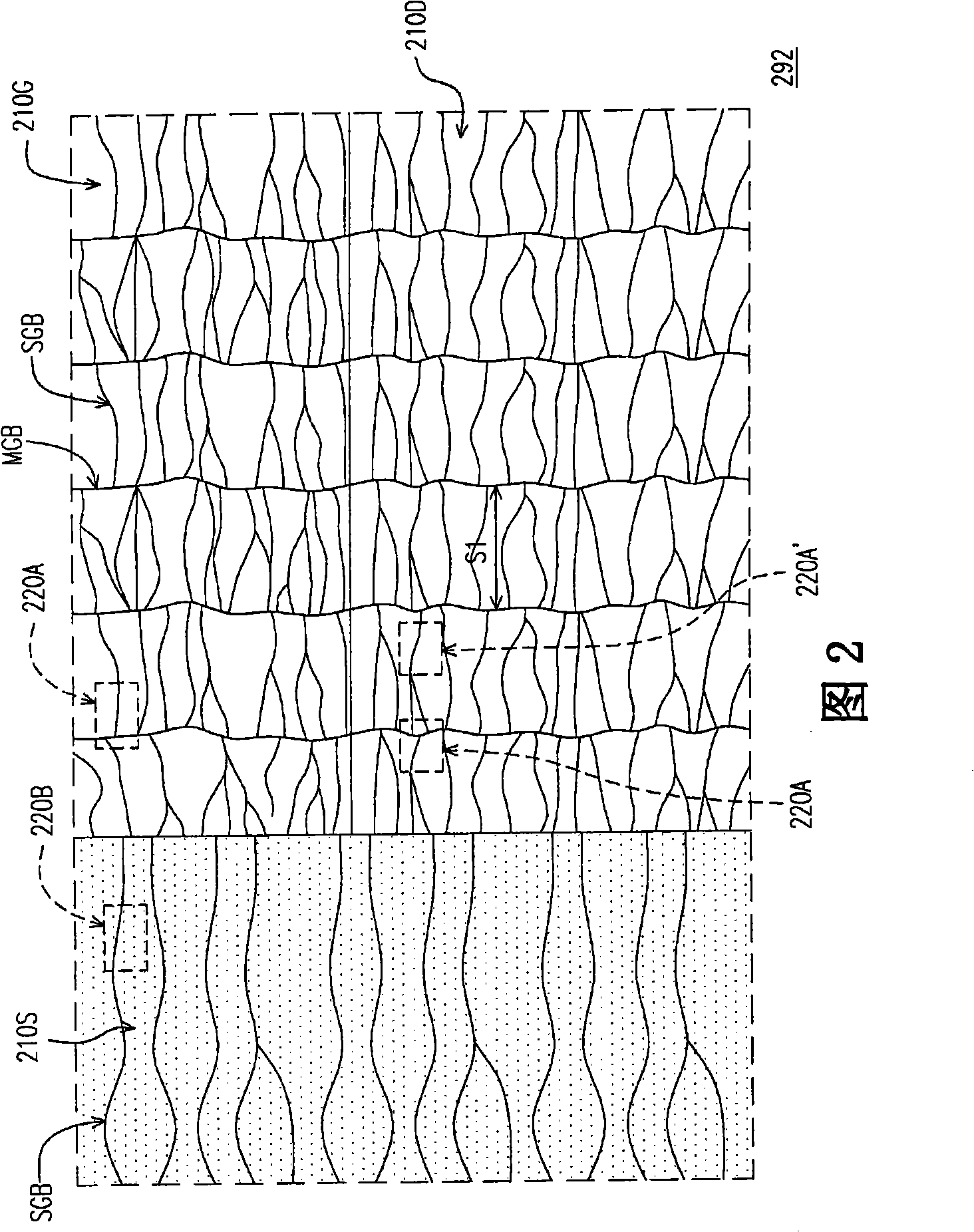
[0081] FIG. 5A is a schematic cross-sectional view of the thin film transistor array substrate according to the second embodiment of the present invention along the lines AA, BB, and CC in FIG. 1A . Please refer to FIG. 5A , for the sake of simplification, the above-mentioned components similar to those mentioned above will not be described again. Compared with the previous embodiments, the second polysilicon island 320B of the thin film transistor array substrate 300 of this embodiment has a main grain boundary MGB and a secondary grain boundary SGB, and the main grain boundary MGB of the second polysilicon island 320B is only located In the source region 222 and / or the drain region 224 , in other words, there is no main grain boundary MGB in the channel region 226 of the second polysilicon island 320B. The formation positions of the main grain boundary MGB and the secondary grain boundary SGB of the second polysilicon island 320B can be controlled, for example, by adjusting ...

no. 3 example

[0085] FIG. 6A is a schematic cross-sectional view of the thin film transistor array substrate according to the third embodiment of the present invention along the lines AA, BB, and CC in FIG. 1A . Please refer to FIG. 6A , for the sake of simplification, the above-mentioned components similar to those described above are not described again. Compared with the second embodiment, the main grain boundary MGB of the second polysilicon island 420B of the thin film transistor array substrate 400 of this embodiment is only located in the source region 222 and / or the drain region 224, in other words, the second most There is no main grain boundary MGB in the channel region 226 of the silicon island 420B. Moreover, in this embodiment, the grain size in the second polysilicon island 420B of the thin film transistor array substrate 400 is substantially smaller than the grain size in the first polysilicon film.

[0086]FIG. 6B is a diagram showing the grain arrangement state of the poly...


PUM


Abstract

The invention provides a substrate for a thin film transistor (TFT) array and a method for manufacturing the same. The substrate for the TFT array comprises the substrate, a plurality of multicrystal silicon islands and a plurality of grid electrodes, wherein the substrate has a display zone, a grid electrode drive zone and a source electrode drive zone; the multicrystal silicon islands are arranged on the substrate, and each multicrystal silicon island has a source electrode zone, a drain electrode zone and a channel zone positioned between the source electrode zone and the drain electrode zone; moreover, the multicrystal silicon islands comprise a plurality of first multicrystal silicon islands and second multicrystal silicon islands, wherein the first multicrystal silicon islands are arranged inside the display zone and the grid electrode drive zone, and have major grain boundaries and minor grain boundaries, and the major grain boundaries is only positioned inside the source electrode zone and / or the drain electrode zone; the second multicrystal silicon islands are arranged inside the source electrode drive zone; the size of grain inside the first multicrystal silicon islands is different from that inside the second multicrystal silicon islands; and the grid electrodes are arranged on the substrate and are corresponding to the channel zone.

Description

technical field [0001] The present invention relates to a semiconductor element array substrate and a manufacturing method of the semiconductor element array substrate, and in particular to a thin film transistor array substrate and a manufacturing method of the thin film transistor array substrate. Background technique [0002] In recent years, with the increasing maturity of optoelectronic technology and semiconductor manufacturing technology, flat-panel displays have flourished. Among them, liquid crystal displays have gradually replaced traditional cathodes based on their advantages of low-voltage operation, no radiation scattering, light weight, and small size. Ray tube displays have become the mainstream of display products in recent years. [0003] In general, liquid crystal displays can be classified into two types: amorphous silicon thin film transistor liquid crystal displays and low temperature poly-silicon thin film transistor liquid crystal displays. Compared w...

Claims


Application Information

Patent Timeline
Patent Type & Authority Applications(China)
IPC IPC(8): H01L27/12H01L21/84G02F1/1362
Inventor 孙铭伟赵志伟
Owner AU OPTRONICS CORP
Why Eureka
Try Eureka