Printed circuit board, design method thereof and terminal product main board

A technology of printed circuit board and design method, applied in the directions of printed circuit, printed circuit, printed circuit manufacturing, etc., can solve the problems of many layers of boards, long processing cycle, technological level limitation, etc., so as to reduce production cost and reduce signal The effect of crosstalk

Active Publication Date: 2009-02-11
HUAWEI TECH CO LTD
View PDF0 Cites 22 Cited by
  • Summary
  • Abstract
  • Description
  • Claims
  • Application Information

AI Technical Summary

Problems solved by technology

[0005] However, the existing six-layer HDI board has a high production cost due to many process steps, long processing cycle, and many layers of boards used.
In addition, the thickness of the six-layer HDI board is not easy to make thin. Due to the large number of layers, a certain insulation strength must be ensured between each layer. The dielectric layer between each signal layer should not be too thin. The yield rate is declining. At present, most PCB manufacturers are limited by the technology level. Usually, the non-laser hole dielectric layer is greater than 4mil. Therefore, the current six-layer first-order HDI board is usually greater than or equal to 0.8mm in thickness. When it is less than 0.8mm, the production cost will increase proportionally.

Method used


Image

  • Printed circuit board, design method thereof and terminal product main board
  • Printed circuit board, design method thereof and terminal product main board
  • Printed circuit board, design method thereof and terminal product main board

Examples


Embodiment approach 1

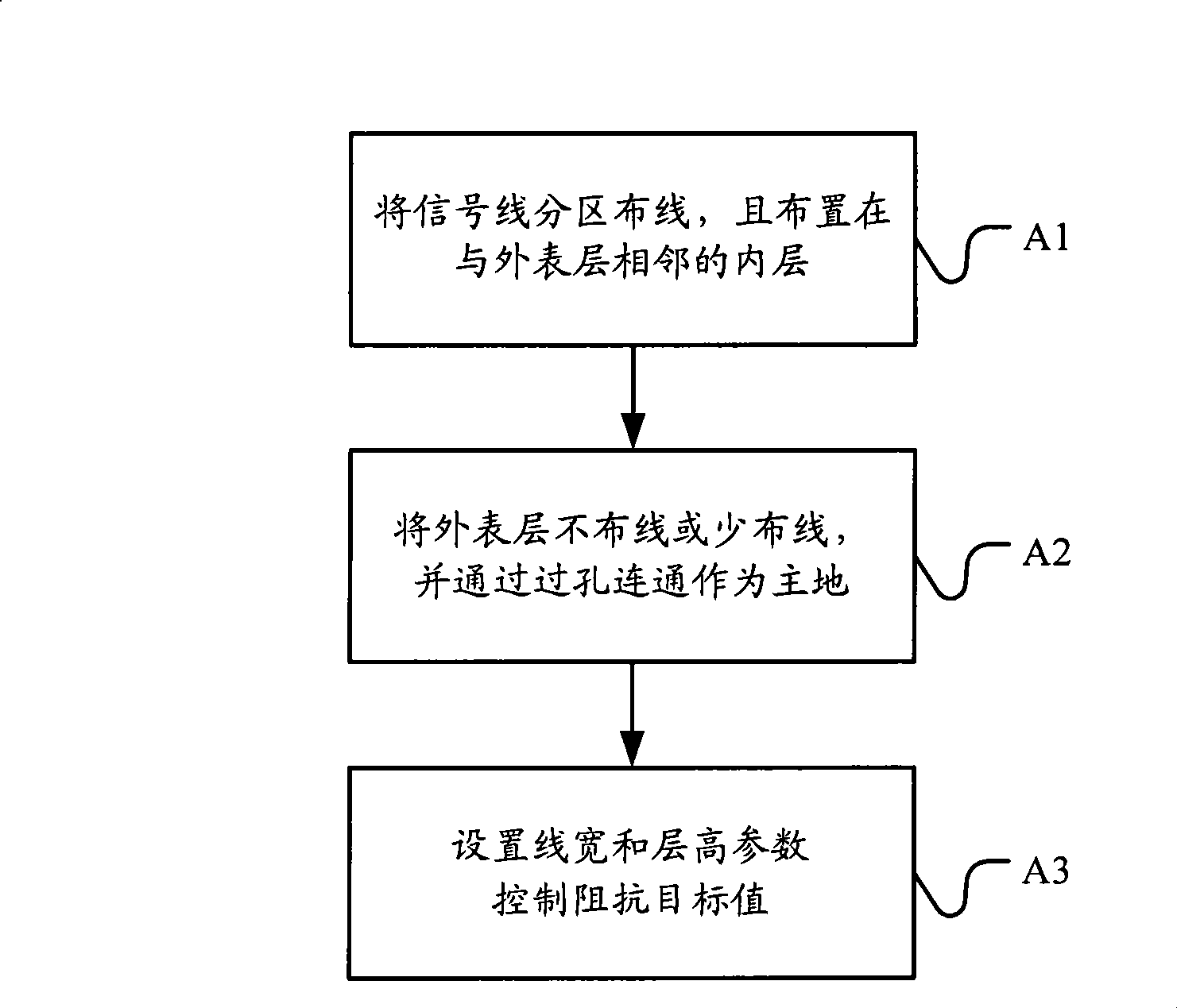
[0047] For the four-layer laser blind hole HDI board designed in the embodiment of the present invention, please refer to Figure 5 , are two outer layers and two inner layers, the two outer layers are the first layer (Layer1) 10 and the fourth layer (Layer4) 40, and the two inner layers are the second layer (Layer2) 20 and the third layer ( Layer3) 30, the circuit board also includes laser blind holes 50, buried holes 60 and via holes 70. The structure shown in this figure is only one of the structural forms of the embodiment of the present invention, and it is only an example for illustration here. Figure 6-11 More structural forms of the four-layer printed circuit board with laser blind vias are schematically shown. The specific technical details are explained below with this preferred embodiment.

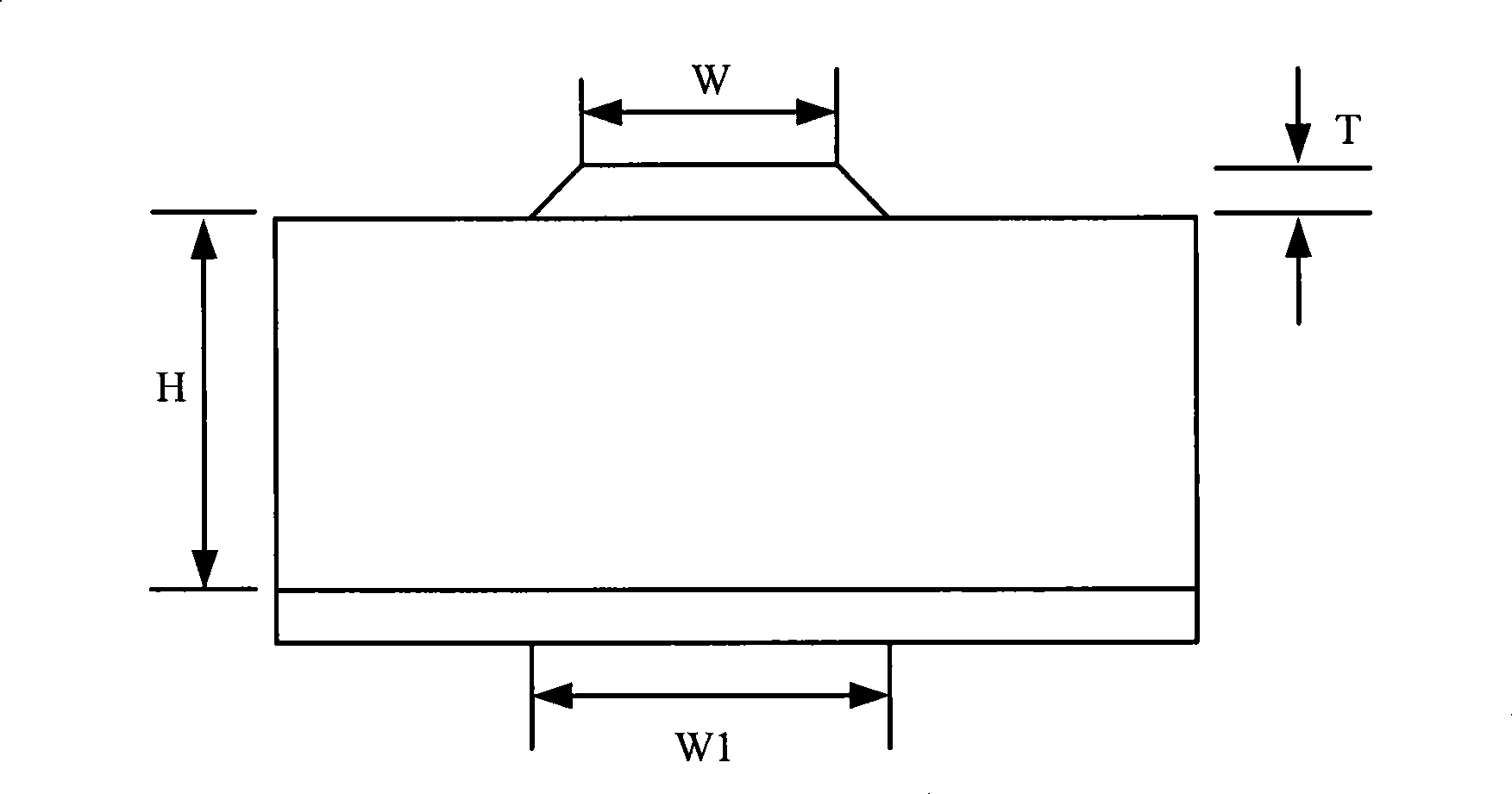
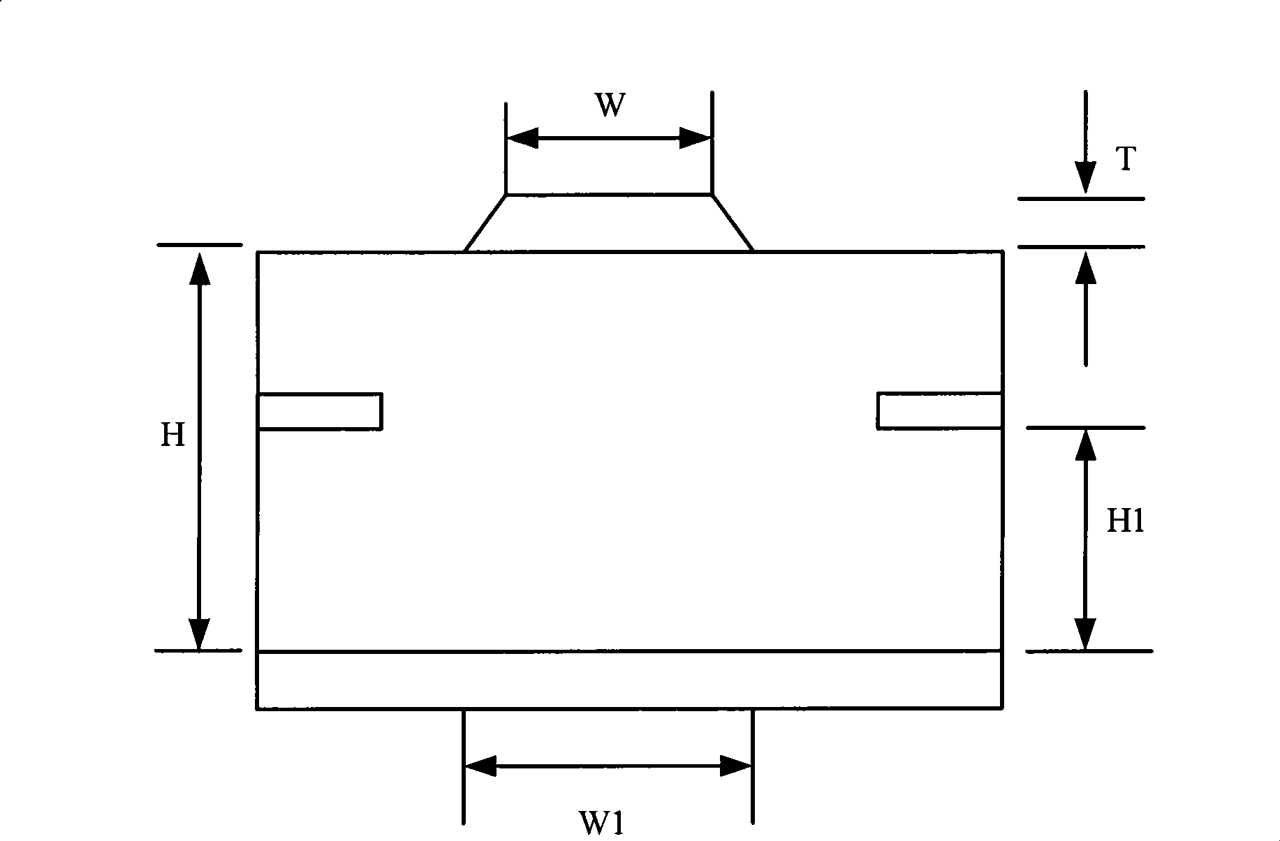
[0048] The specific parameters of the laminated design of the four-layer laser blind via HDI board are shown in Table 1 below.

[0049]

[0050]

[0051] ...

Embodiment approach 2

[0147] For the four-layer mechanical blind hole PCB board designed in the embodiment of the present invention, please refer to Figure 12 , are two surface layers and two inner layers, the two surface layers are the first layer (Layer1) 10 and the fourth layer (Layer4) 40, and the two inner layers are the second layer (Layer2) 20 and the third layer (Layer3) 30. The circuit board further includes blind holes 50 and through holes 70. The structure shown in this figure is only a structural form in the four-layer mechanical blind hole PCB board in the embodiment of the present invention, and it is only an example here. Figure 13-15 More structural forms of a four-layer mechanical blind hole PCB board are shown.

[0148] The specific technical details specific to the four-layer mechanical blind hole PCB board are explained below with this preferred embodiment. For other technical details, please refer to the specific implementation of the four-layer laser blind via HDI board. ...


PUM


Abstract

The embodiment of the invention discloses a design method of a printed circuit board. The method comprises the following steps of laying a signal wire on inner layers next to an outer surface layer by zones; not wiring the outer surface layer or laying less wire on the outer surface layer which is used as a main area communicated through a hole; and setting wire width and layer height parameters to control an impedance target value. Correspondingly, the embodiment of the invention provides the printed circuit board, which comprises the out surface layer, and two inner layers positioned between the surface layers. The inner layers next to the out surface layer are used for laying signal wires by zones. Few wires or no wire is laid on the out surface layer and the outer surface layer is used as the main area communicated through the hole. The invention also discloses a terminal product main board using the printed circuit board. The technical proposal provided by the embodiment of the invention can reduce the cost and improve the reliability by layer reduction design under the condition that the basic properties of the original multi-layer printed circuit board is kept.

Description

[0001] This application claims the priority right of the Chinese invention patent application filed on March 23, 2007 with the application number 200710090909.0 and the title "printed circuit board and its design method". technical field [0002] The invention relates to printed circuit board technology, in particular to a multilayer printed circuit board and a design method thereof. The invention also relates to a terminal product main board using the printed circuit board. Background technique [0003] Printed circuit board PCB (printed circuit board) is a structural component formed by insulating materials supplemented by conductor wiring. It is used in various communication and electronic equipment. Its technology is also developing continuously, from the original single panel to double panel. Panels, and then developed to multi-layer boards, currently four- and six-layer boards are widely used. HDI (high density interconnection) technology is the development trend of p...

Claims


Application Information

Patent Timeline
Patent Type & Authority Applications(China)
IPC IPC(8): H05K1/00H05K3/46
CPCH05K3/429H05K2201/09627H05K3/4602H05K1/0218H05K1/025H05K2201/09536H05K2201/0715H05K2201/0191H05K1/0298H05K1/0237
Inventor 沈晓兰叶青松魏孔刚
Owner HUAWEI TECH CO LTD
Why Eureka
Try Eureka