Construction of surface conductive field emission electronic source conductive film

A technology of conductive film and electron source, applied in the direction of cathode ray tube/electron beam tube, discharge tube/lamp components, circuits, etc., can solve the problems of low emission current density, low electron emission rate, and low brightness of SED, and achieve The effect of increasing emission current density and electron emission rate, high carrier mobility, and low threshold voltage

Inactive Publication Date: 2009-03-11
XI AN JIAOTONG UNIV
View PDF0 Cites 2 Cited by
  • Summary
  • Abstract
  • Description
  • Claims
  • Application Information

AI Technical Summary

Problems solved by technology

[0010] The advantage of the SED using palladium oxide as the conductive film is that the stability of electron emission is good, but the disadvantage is that the emission current density and electron emission rate are low, resulting in low brightness of the SED

Method used


Image

  • Construction of surface conductive field emission electronic source conductive film
  • Construction of surface conductive field emission electronic source conductive film
  • Construction of surface conductive field emission electronic source conductive film

Examples


Embodiment Construction

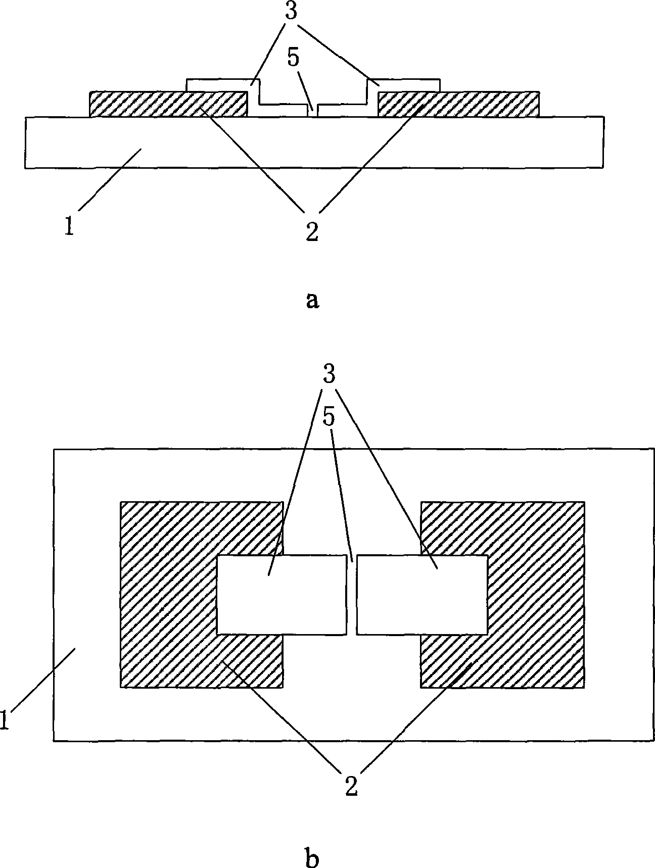
[0029] refer to figure 1 As shown, the manufacturing process of the conductive film is to make the PdO film 3 on the glass substrate 1 with the device electrode 2 and other components, so the conductive film is a single-layer material film, and then the film is "formed with power" process to obtain the gap 5.

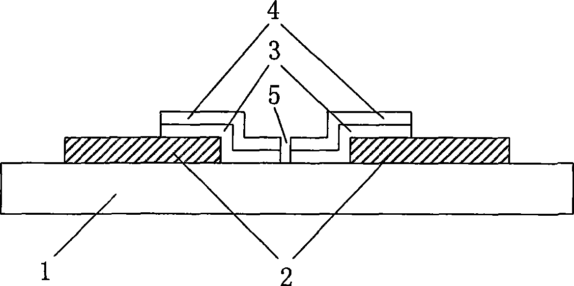
[0030] refer to figure 2 As shown, the manufacturing process of the conductive film is to first make a palladium oxide PdO film 3 on a glass substrate 1 with components such as device electrodes 2, and then make an amorphous carbon film 4 on it, thereby forming two layers of PdO-amorphous carbon structure conductive film, and finally perform the process of “power-on formation” on the film to obtain the gap 5 .

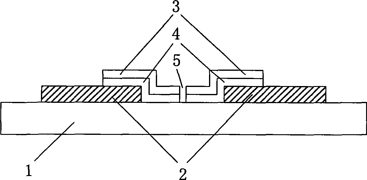
[0031] refer to image 3 As shown, the manufacturing process of the conductive film is to first make an amorphous carbon film 4 on a glass substrate 1 with components such as device electrodes 2, and then make a palladium oxide PdO film 3 on it, thereby form...


PUM


Abstract

The invention discloses a conducting film structure of a surface conduction field emission electron source, namely, a conducting film of an electron source is formed by a multilayer composite film which is formed by a palladium oxide film (PdO) and an amorphous carbon film, the electron transmitting performance of the conducting film can be improved by using the good electron emission stability of the palladium oxide film and the lower effective work function, the large carrier mobility, the high breakdown voltage, the wide forbidden bandwidth and the high heat conduction coefficient of the amorphous carbon film, and consequently, the emission current density and the electron emissivity of the field emission electron source are increased.

Description

technical field [0001] The invention belongs to the field of flat panel display device manufacturing, and relates to a structure of an electron emission source, in particular to a layer structure of a conductive film of a surface conduction electron emission source that can be used in a field emission display device. Background technique [0002] Surface-conduction Electron-emitter Display (SED) is an advanced flat panel display device newly developed in recent years. No matter in terms of contrast, gray scale, color and dynamic image display quality, etc., or in terms of power consumption and thickness, SED is better than the current mainstream liquid crystal display (LCD) and plasma display (PDP), and is considered to be the successor The next generation of flat panel display devices after LCD and PDP. [0003] SED is a high-vacuum display device. It consists of a front glass substrate, a rear glass substrate, and a surrounding sealing material frame to form a sealed stru...

Claims


Application Information

Patent Timeline
Patent Type & Authority Applications(China)
IPC IPC(8): H01J29/04H01J1/304
Inventor 胡文波吴胜利刘纯亮张劲涛王文江孙永亮
Owner XI AN JIAOTONG UNIV
Why Eureka
Try Eureka