Carbon-metal nano-composite materials for field emission cathodes and devices

Inactive Publication Date: 2005-05-10
NANODYNAMICS INC
View PDF17 Cites 12 Cited by
  • Summary
  • Abstract
  • Description
  • Claims
  • Application Information

AI Technical Summary

Benefits of technology

[0012]The proposed approach takes advantage of the tailorable properties of this unique coating, which consists of an amorphous diamond-like and quartz-like structure “doped” with controlled quantities of metals (Me-DL ASC). Me-DL ASC appears as a new composition of matter that allows formation of special composites at atomic level with properties that range from highly conductive to purely dielectric. Metal components imbedded in the host matrix in an appropriate way create three-dimensional random conductive structures spreading in the film as metal fibers. The fibers can be made very thin, in the range of one to a few nm. When exposed to the vacuum, they can serve as multiple, extremely efficient electron emission sites. Since the emitter surface curvature essentially controls the emission efficiency, one can expect very low emission threshold voltage from the metal network, significantly lower than that in traditiona, Spindt, metal tip cathodes. In addition, as this material belongs to the diamond-like family, DL ASC has a potential to posses low work function or even negative electron affinity. Finally, this material can be formed as a highly stable super-lattice containing alternating DL ASC and Me-DL ASC layers with the minimum thickness being about 2 nm.
[0013]DL ASC also exhibits high chemical, mechanical, thermal and radiation stability, together with excellent adhesion to a wide variety of substrates with minimal interface thickiess and intrinsic stress, which warrant long lifetime for field emission cathodes and devices.
[0014]In consideration of the forgoing, an object of the present invention is the field emission material with multiple emission sites, high field enhancement factor, potentially low work function and appears as highly adherent, thermally, chemically and mechanically stable material.

Problems solved by technology

Two important limitations of micro-fabricated field emitter tips are their poor reliability and stability.
In large part, these limitations can be traced to the inherent chemical / thermodynamic instability of clean, highly curved surfaces.
Conventional fabrication processes, combined with the usual operating conditions inevitably lead to the build up of contaminants on emitter surfaces acting as barriers for electrons resulting in formation of a large effective work function.
Another problem with the tip cathodes originates from a mechanical damage of the tips by positively charged ions, which reduces the cathode lifetime.
However, during cathode operation, graphite inclusions appear to act as nucleation sites to induce further conversion of diamond to graphite, which leads to material degradation.
In addition, it is very difficult to attain uniform emission with minimum cathode series resistance, which is important for application of this technology to high luminance / large format displays.
The carbon filaments stemming from the carbon film represent good electric field concentrators yielding emission threshold as low as 1 V m. The drawbacks of this approach are that the technology is non-planar and cannot use the photolithography processing.
The resultant control voltages are typically in the range of hundreds voltage, which makes difficult utilizing this technology for micro-devices.
Second, the edge is much more resistive to a mechanical damage.

Method used


Image

  • Carbon-metal nano-composite materials for field emission cathodes and devices
  • Carbon-metal nano-composite materials for field emission cathodes and devices
  • Carbon-metal nano-composite materials for field emission cathodes and devices

Examples


Embodiment Construction

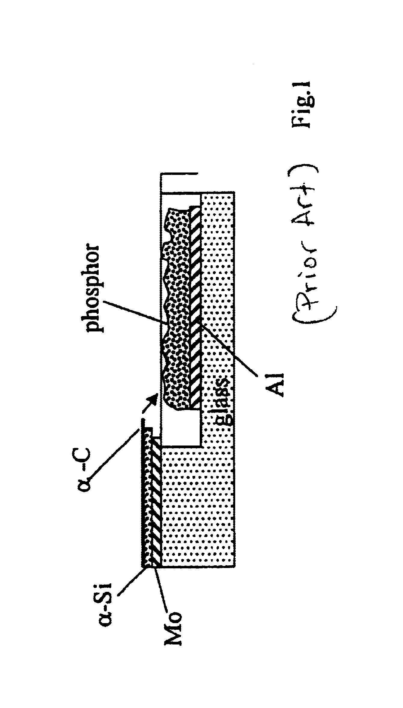
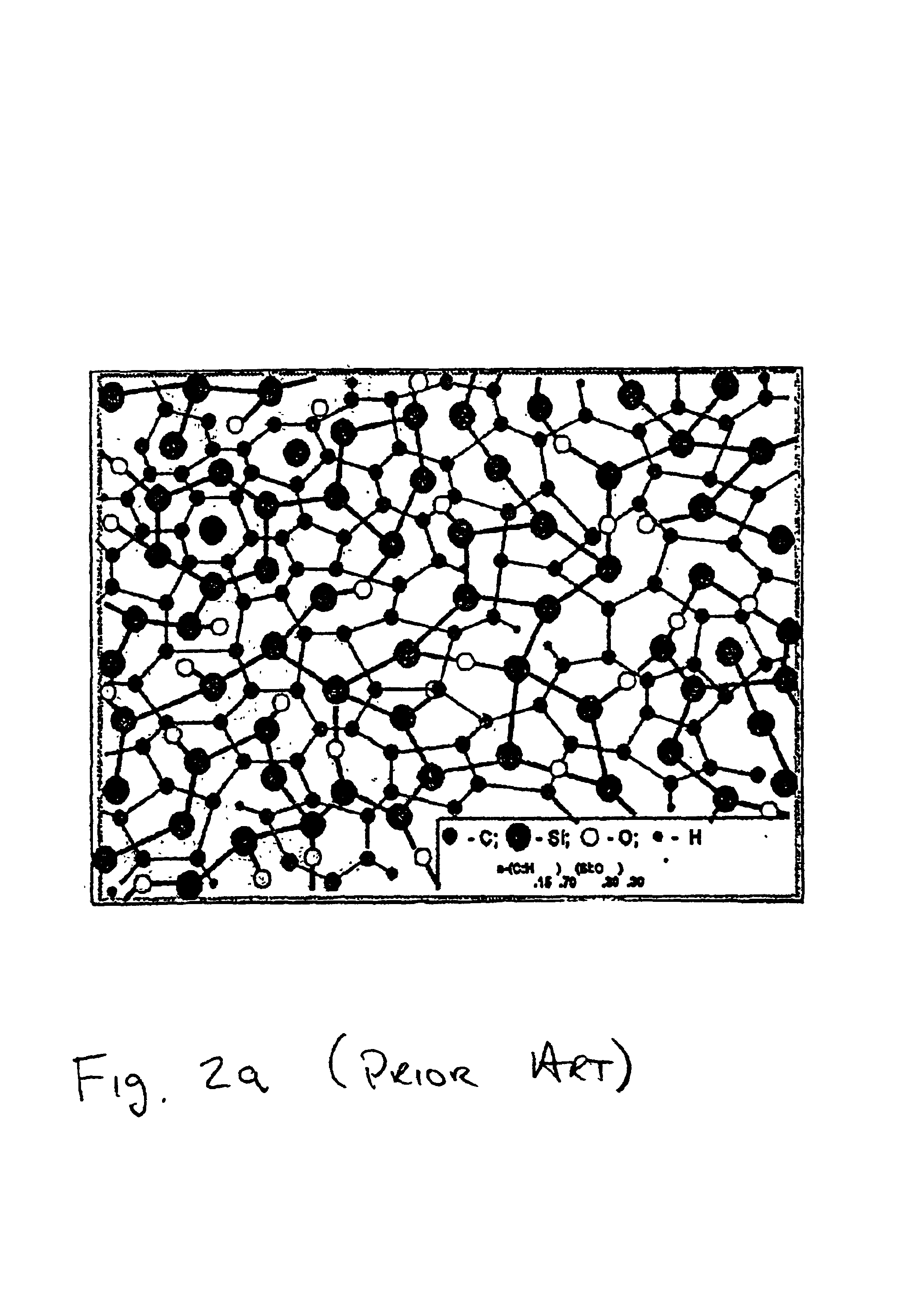
[0041]FIG. 2 is an example of diagrams of atomic-scale composites structure and structures (Prior Art). The fundamental structure of the atomic-scale composites to be implemented as the field emission cathodes is comprised of two interpenetrating random networks. The first basic network consists of material capable of a low voltage emission, while the second is stabilizing dielectric network. An example of such structures are DL ASC, that belong to the diamond-like family of materials. There two major class of DL ASC. The first class of DL ASC consists of a random carbon network, mainly in the form of sp3 “diamond-like” bonds chemically stabilized by hydrogen atoms, and a quartz-like silica random network, e.g. silicon network chemically stabilized by oxygen atoms. These interpenetrated networks form together a purely amorphous structure (FIG. 2, a). Such two-network DL ASC does not contain any clusters or ordering greater than that defined by one third of the radius of the coordina...


PUM

PropertyMeasurementUnit
Percent by atomaaaaaaaaaa
Areaaaaaaaaaaa
Nanoscale particle sizeaaaaaaaaaa

Abstract

A field emission cathode consisting of atomic-scale composite material comprising three atomic networks is proposed. The first and the second atomic networks penetrate into each other and form carbon-based stabilized dielectric medium and the third atomic network is a conductive network of metallic atoms. The atomic scale composite material may also contain conductive nano-crystals immersed into the carbon-based stabilized dielectric medium. The atomic-scale conductive network and nano-crystals reach the film surface and film edge forming nanometer scale field emission sites. They may be partially exposed by etching the other components of the cathode material thereby forming atomic-scale and / or nano-scale field emission metallic tips.The field emission cathode can be used as an efficient cold cathode in a variety of electronic devices, such as flat panel field emission displays, microwave diodes, triodes and more complex devices.

Description

BACKGROUND OF THE INVENTION[0001]1. Field of the Invention[0002]The invention relates to electric field induced electron emitters and more particularly, to field emission cathodes and related micro-electronic devices and field-emission displays based on the use of carbon-metal diamond-like composites materials.[0003]2. Background Art[0004]The interest to advanced field emission (FE) cathode materials arises from a number of applications including field emitters for microelectronic devices, flat panel displays, high intensity electron beams for accelerators and free electron lasers, and high current density cathodes for microwave power tubes, klystrons and gyrotrons. As compared with more conventional thermionic electron sources, cold FE cathodes require no heater circuit and are capable of generating high current densities.[0005]The most common approach in concentrating electric field to create the field induced electron emission is fabrication of metal tips using geometry dependent...

Claims


Application Information

Patent Timeline
IPC IPC(8): H01J1/304H01J1/30
CPCB82Y10/00H01J1/3046Y10T428/30H01J2201/30469
Inventor DORFMAN, BENJAMIN F.
Owner NANODYNAMICS INC
Why Eureka
Try Eureka