Apparatus for manufacturing aspherical microlens array

A technology of microlens arrays and manufacturing devices, which is applied in the fields of lenses, optics, instruments, etc., can solve the problems that microlenses cannot control the lens surface shape, and cannot detect the lens surface shape and optical performance in real time, so as to achieve good focusing and imaging performance, The effect of high repeatability and simple production process

Inactive Publication Date: 2010-06-02
UNIV OF SCI & TECH OF CHINA
View PDF4 Cites 2 Cited by
  • Summary
  • Abstract
  • Description
  • Claims
  • Application Information

AI Technical Summary

Problems solved by technology

[0006] In order to solve the problem that the existing microlens and its array device cannot be manipulated in the lens surface shape, and the lens surface shape and optical performance cannot be detected in real time, the present invention provides an aspheric surface with simple process, high repeatability and low manufacturing cost Microlens Array Fabrication Device

Method used


Image

  • Apparatus for manufacturing aspherical microlens array
  • Apparatus for manufacturing aspherical microlens array
  • Apparatus for manufacturing aspherical microlens array

Examples


Embodiment

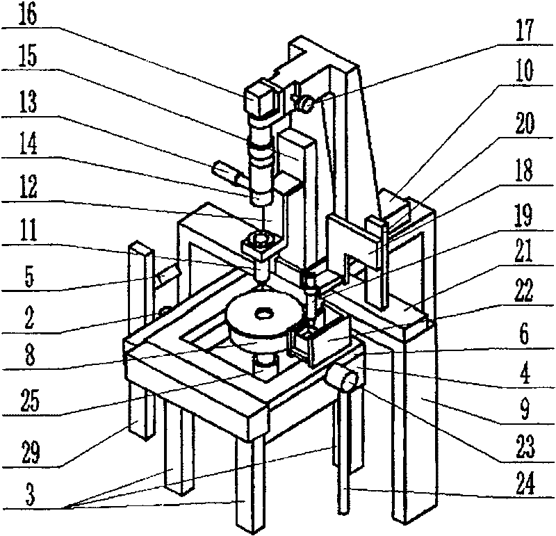
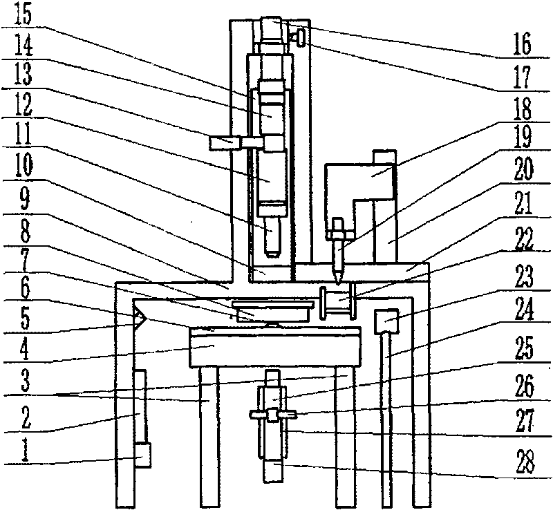
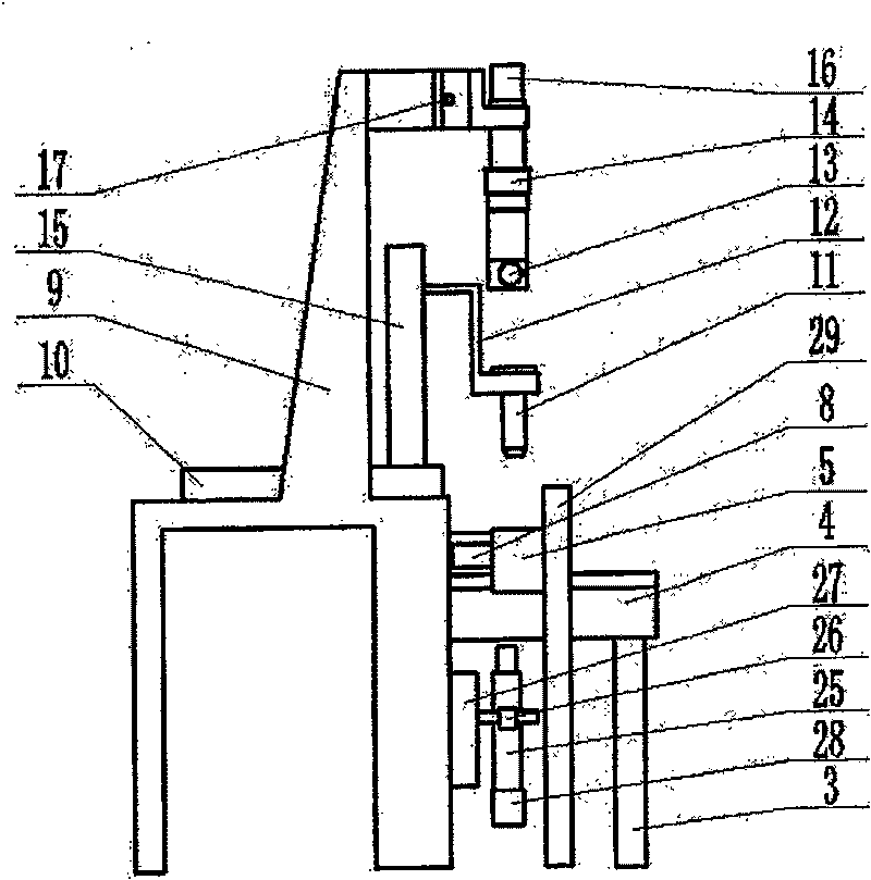
[0035] see figure 1 , figure 2 and image 3 , an aspheric microlens array manufacturing device includes a main frame 9, a syringe 19, an upper electrode 11, a transverse detection optical path, a longitudinal detection optical path, an annular ultraviolet light source 8 and an integral two-dimensional translation stage 4.

[0036] The lower part of the main body support 9 is a workbench shape, and the middle part of the workbench is a door-shaped vertical vertical arm upwards, and the upper end of the vertical vertical arm is a cantilever;

[0037] The syringe 19 is fixed on the syringe longitudinal translation platform 20 through the syringe bracket 18, the syringe longitudinal translation platform 20 is fixed on the syringe transverse translation platform 21, and the syringe 19 is driven by the syringe transverse translation platform 21 and the syringe longitudinal translation platform 20 to move horizontally and vertically in two dimensions , the syringe lateral translat...


PUM

PropertyMeasurementUnit
emission peakaaaaaaaaaa

Abstract

The invention relates to a non-sphere micro-lens array manufacturing device, which solves the problem that during the manufacture of the prior micro-lens and array devices thereof, the surface shape of the micro-lens is beyond control and real-time detection of optical performance of the surface of the micro-lens is impossible. The device comprises a main support, an injector, an upper electrode,a transverse detection optical circuit, a longitudinal detection optical circuit, an annular, an ultraviolet source and so on, wherein a liquid box is arranged under the injector, and one side of theinjector is provided with the upper electrode and a specimen stage. An undersurface of the specimen stage and an upper surface of the upper electrode are provided with tin indium oxide coatings to form a parallel-plate capacitor type electric field. The injector injects a liquid drop between the specimen stage and the upper electrode, the electric filed controls the surface shape of the liquid lens, the transverse detection optical circuit carries out real time detection of the surface shape of the liquid lens, the longitudinal detection optical circuit detects a focused spot, aberration analysis is carried out according to the surface shape and an image of the focused spot and the annual ultraviolet source solidifies the liquid lens when proper surface shape and focused spot are proper, so a solid non-sphere micro-lens with excellent optical performance is obtained. The device has the advantages of simple process, high repetitiveness and low cost.

Description

technical field [0001] The invention relates to a microlens array manufacturing device, in particular to a microlens array manufacturing device capable of changing the lens surface shape and detecting lens optical parameters in real time. Background technique [0002] Microlens is one of the important devices in the field of micro optics. Microlens and its array devices are widely used in beam shaping, beam coupling, fly eye lens, integrated imaging and other fields. [0003] At present, the common production methods of microlens mainly include diamond cutting method, photoresist hot-melt molding method, compression molding method, inkjet printing technology, etc. The diamond cutting method is to cut the glass by machining to obtain the lens refracting surface. The surface finish of the lens obtained by this method is not high, and the cost is high, and the process repeatability is poor. The photoresist hot-melt molding method is to obtain a block-shaped photoresist by phot...

Claims


Application Information

Patent Timeline
Patent Type & Authority Patents(China)
IPC IPC(8): B29C41/12B29C41/52B29C41/36B29C41/46G02B13/00G02B3/02B29L11/00
Inventor 王克逸詹珍贤姚海涛丁志中李端发
Owner UNIV OF SCI & TECH OF CHINA
Why Eureka
Try Eureka