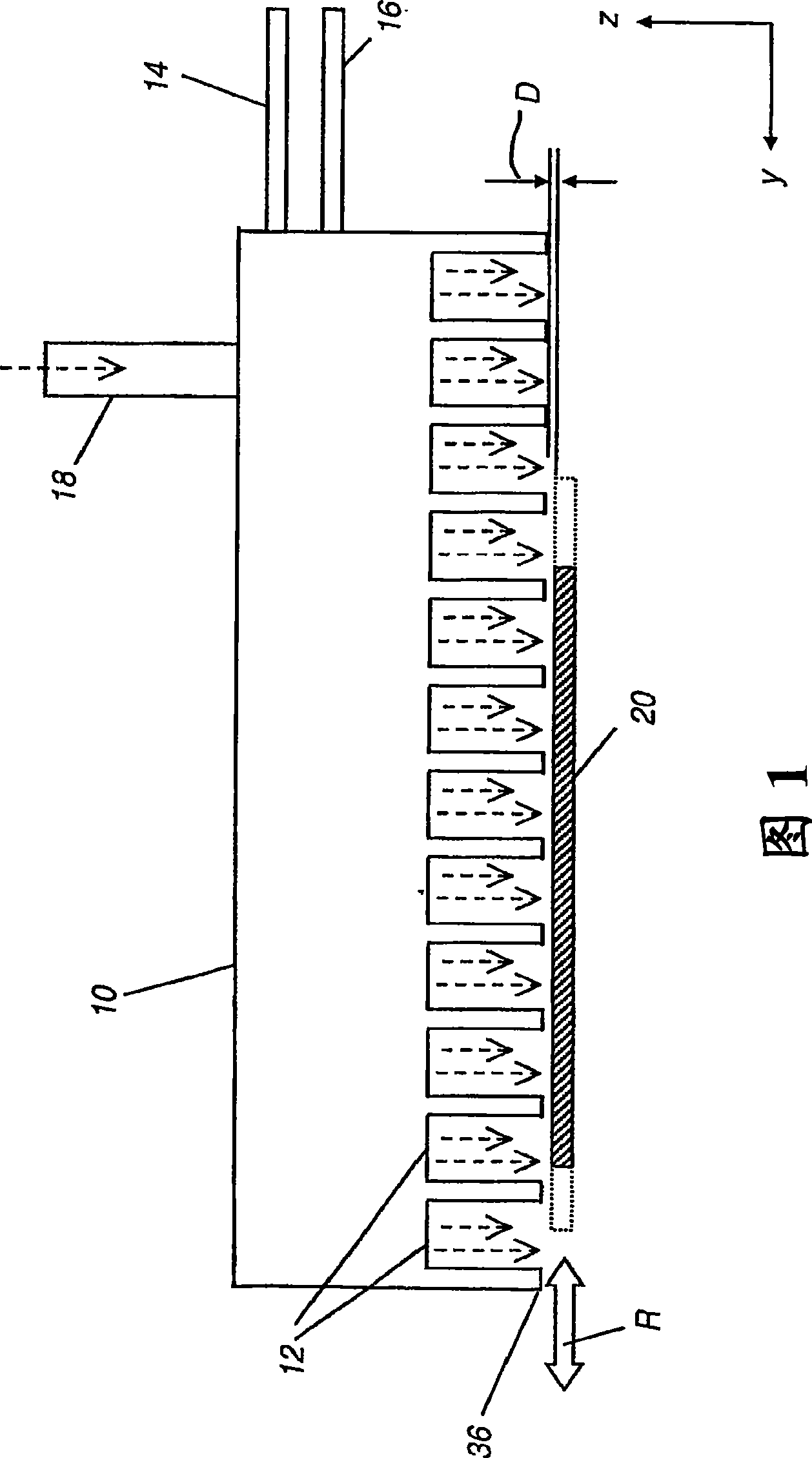
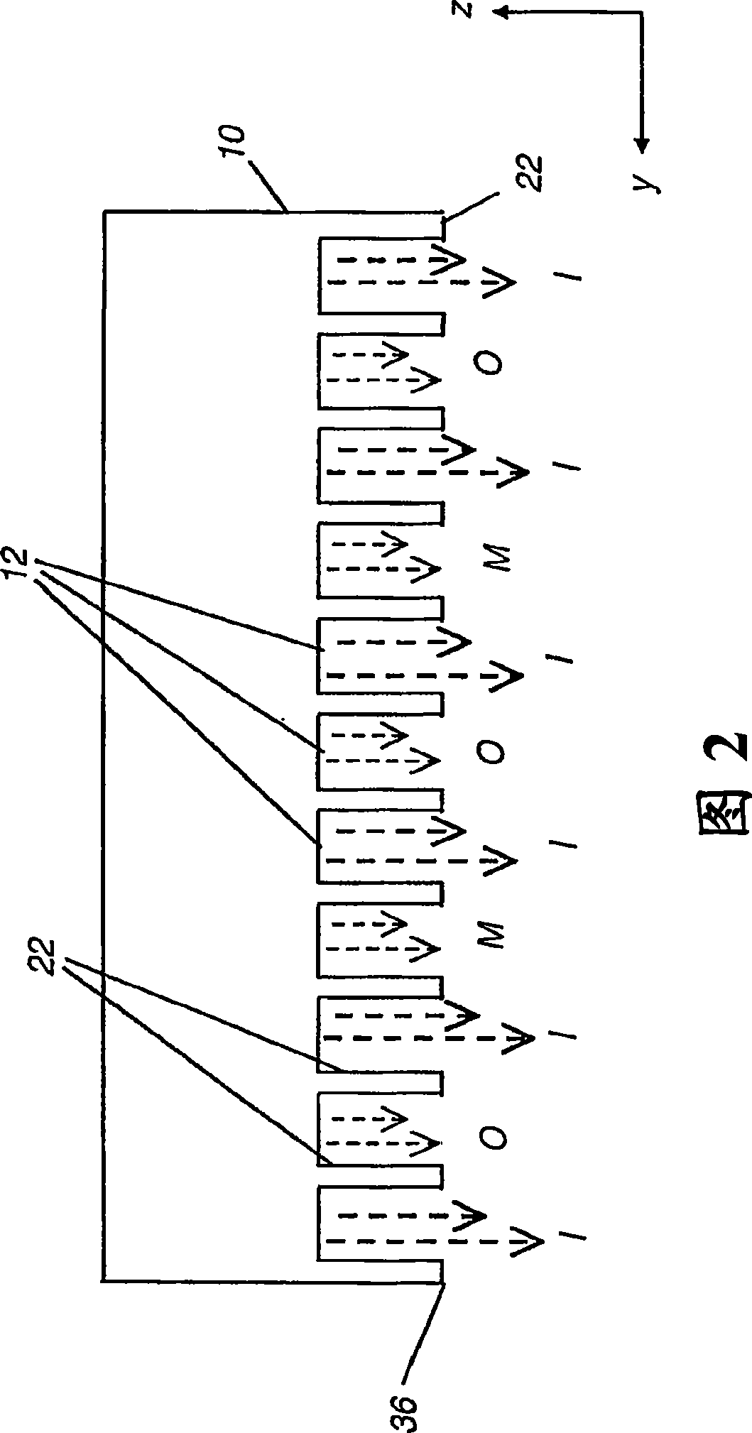
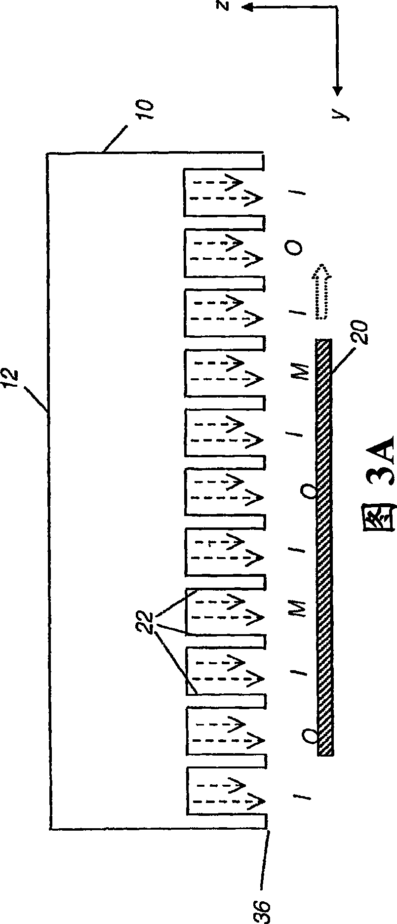
Apparatus for atomic layer deposition
一种沉积装置、沉积系统的技术,应用在涂层、金属材料涂层工艺、气态化学镀覆等方向,能够解决小获得ALD气体分配装置、不易灵活性等问题,达到紧凑装置的效果
- Summary
- Abstract
- Description
- Claims
- Application Information
AI Technical Summary
Problems solved by technology
Method used
Image
Examples
Embodiment 1
[0143] This example illustrates the manufacture of the zinc oxide semiconductor thin film of the present invention for manufacturing a working thin film transistor. In this structure, the gate of the device is a heavily doped silicon wafer, and the insulator is a silicon dioxide film grown by thermal processing on the silicon wafer before depositing a zinc oxide semiconductor film.
[0144] The zinc oxide semiconductor layer is applied with the deposition system of the present invention. Two tests were performed with a substrate temperature of 200°C and the following conditions:
[0145] Table 1
[0146]
sample Diethylzinc
bubbler flow
(sccm) metal precursor
dilution flow
(sccm) air flow
(sccm) water bubbler flow
(sccm) oxidizing agent
dilution flow
(sccm) Nitrogen
purge flow
(sccm)
cycle 1-A 10 620 5 10 1000 1500 40 1-B 5 620 5 5 1000 1500 40
[0147] After depositing ZnO, aluminum con...
Embodiment 2
[0152] This example illustrates the fabrication of aluminum oxide thin films of the present invention, showing that high quality insulating films with excellent breakdown voltage can be fabricated. In this structure, a bare silicon wafer is used as an electrode, and an aluminum oxide film is grown on the electrode by the above-mentioned apparatus of the present invention.
[0153] Aluminum oxide layers were applied with substrates deposited at 200°C and below, where 2-B is a repeated data point.
[0154] table 3
[0155]
sample Trimethylaluminum
bubbler flow
(sccm) metal precursor
dilution flow
(sccm) air flow
(sccm) water bubbler flow
(sccm) oxidizing agent
dilution flow
(sccm) Nitrogen
purge flow
(sccm)
cycle 2-A 10 620 10 10 1100 1500 100 2-B 10 620 10 10 1100 1500 100 2-C 10 620 10 10 1100 1500 200 2-D 20 620 10 20 1100 1500 100
[0156]After alumina deposition,...
Embodiment 3
[0161] This example illustrates the use of heavily doped silicon as the gate material, followed by Al 2 o 3 Working transistor devices were fabricated using ZnO as the dielectric and the semiconductor, wherein the latter two species were deposited using the present invention.
[0162] Aluminum oxide films are first deposited according to the following conditions:
[0163] table 5
[0164]
[0165] After alumina deposition, two samples were coated with ZnO using the above setup according to the following conditions:
[0166] Table 6
[0167] Diethylzinc
[0168] Thin film transistors were obtained with 50 μm channel length and 500 μm channel width by evaporating aluminum contacts on the resulting multilayer device through a shadow mask. The results for the device are shown below:
[0169] Table 7
[0170]
[0171] The above data show that by depositing all critical layers with the apparatus of the present invention, high quality thin film tra...
PUM
 Abstract
Description
Claims
Application Information
 - R&D
- Intellectual Property
- Life Sciences
- Materials
- Tech Scout
- Unparalleled Data Quality
- Higher Quality Content
- 60% Fewer Hallucinations
Browse by: Latest US Patents, China's latest patents, Technical Efficacy Thesaurus, Application Domain, Technology Topic, Popular Technical Reports.
© 2025 PatSnap. All rights reserved.Legal|Privacy policy|Modern Slavery Act Transparency Statement|Sitemap|About US| Contact US: help@patsnap.com


