Bipolar junction transistor

A bipolar junction, transistor technology, used in transistors, semiconductor devices, electrical components, etc., can solve problems such as high breakdown voltage, achieve high breakdown voltage, improve common emitter current gain, and enhance transportation capacity. Effect

Inactive Publication Date: 2009-05-06
UNIV OF ELECTRONICS SCI & TECH OF CHINA
View PDF0 Cites 18 Cited by
  • Summary
  • Abstract
  • Description
  • Claims
  • Application Information

AI Technical Summary

Problems solved by technology

The new BJT device structure that has not been publicly reported can greatly improve the current gain and at the same time have a higher breakdown voltage

Method used


Image

  • Bipolar junction transistor
  • Bipolar junction transistor
  • Bipolar junction transistor

Examples


Embodiment Construction

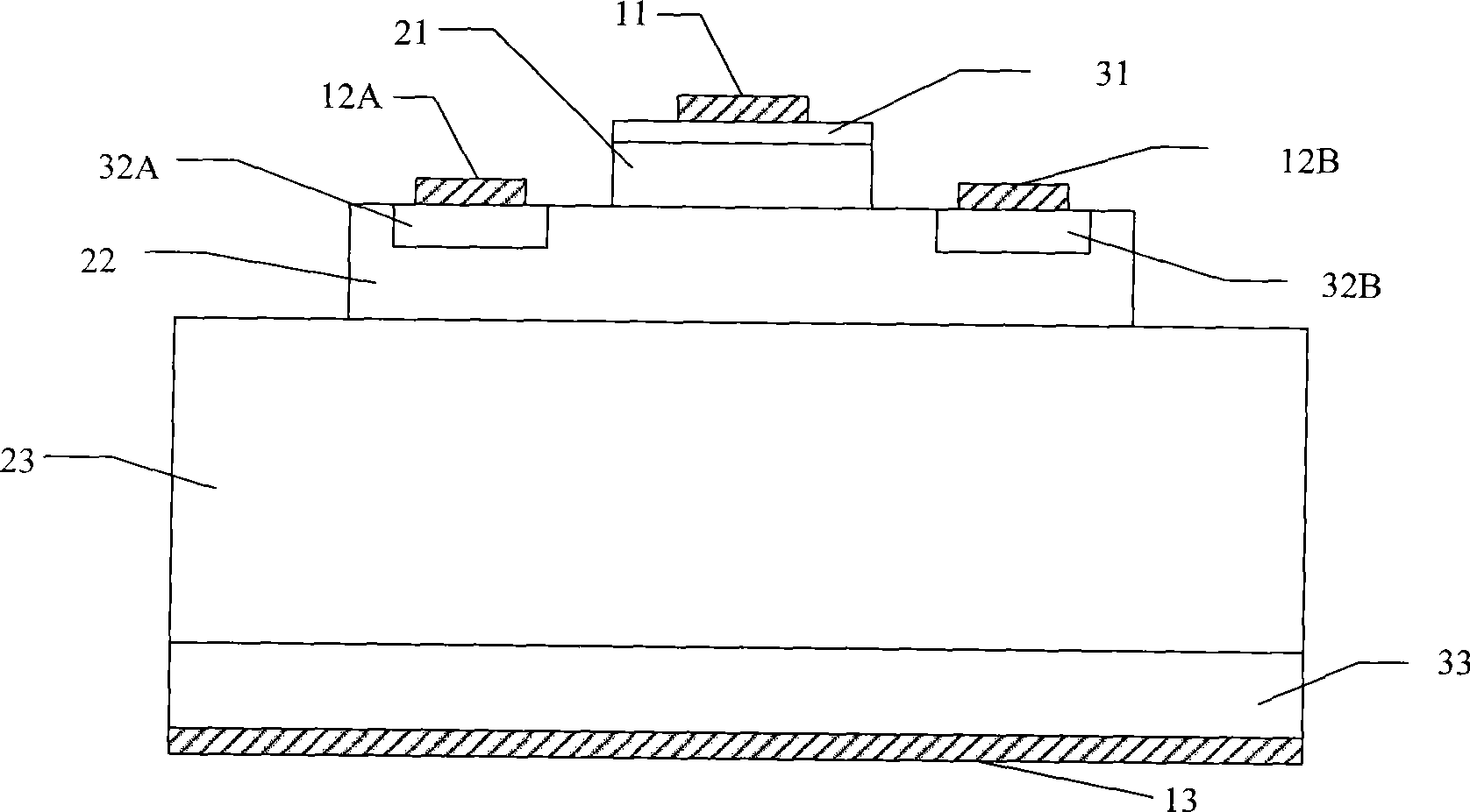
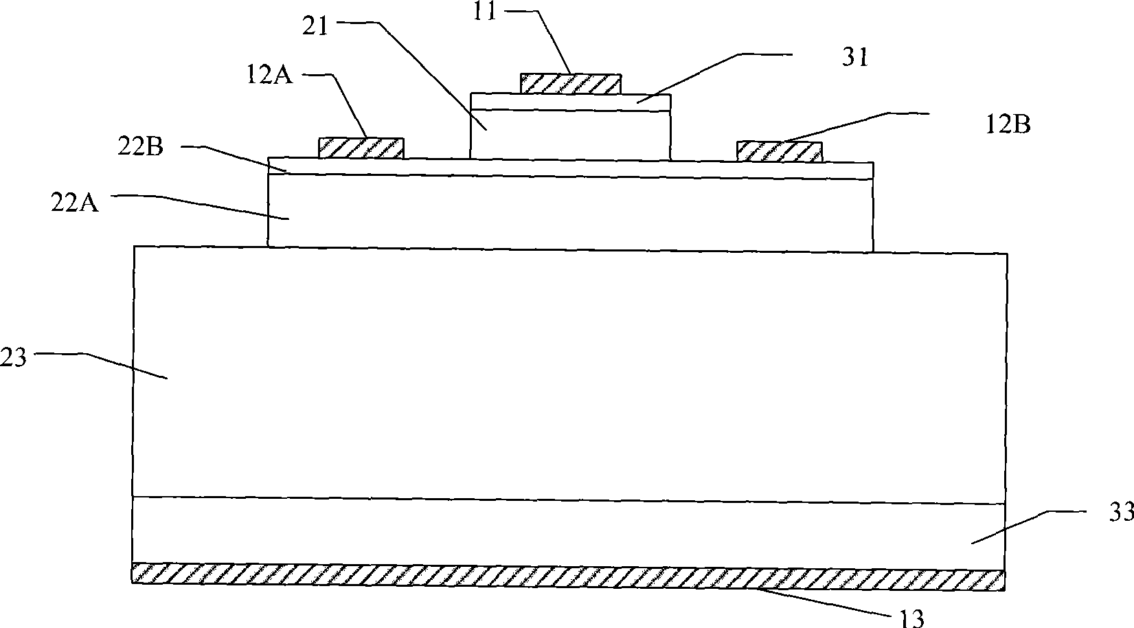
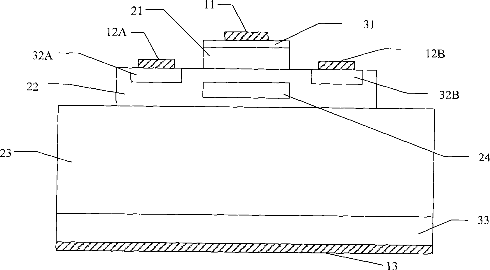
[0019] The invention provides a BJT device with a floating buried layer structure in the base area. Adding a floating buried layer through the base area introduces a new P-N junction, thereby generating a built-in electric field inside the base area. Under the action of the built-in electric field, the transport capacity of the minority carriers in the base region is significantly enhanced, the recombination current in the base region is reduced, and the collector current is increased. At the same time, the floating buried layer in the base region has a modulation effect on the terminal electric field at the base-collector region etching, thereby greatly improving the common-emitter current gain of the device without affecting the breakdown voltage of the device.

[0020] The factors affecting the common emitter current gain of SiC BJT can be divided into three aspects: 1) the recombination effect of the emitter junction space charge region 2) the concentration effect of the e...


PUM


Abstract

A bipolar junction transistor relates to the technical field of a semiconductor power device. The transistor comprises an underlay, a collecting region, an emitting region, a base region, an emitting electrode, a base electrode and a collecting electrode. The transistor is characterized in that a floating buried layer is arranged inside the base region; and the materials of the floating buried layer are different from that of the base region. The invention has the advantages of both good direct current characteristic and breakdown characteristic, namely both high current gain and higher breakdown voltage, and can be widely applied to the field of high-power converters (such as DC-DC converter and inverter).

Description

technical field [0001] The invention relates to the technical field of semiconductor power devices, more specifically, to a high-power bipolar junction transistor (Bipolar Junction Transistor, BJT). Background technique [0002] In recent years, with the rapid development of microelectronics technology and the urgent needs of automotive electronics, aerospace, industrial control, power transportation and other related fields, the development of new high-power semiconductor devices has attracted more and more attention. Among them, the introduction of wide bandgap semiconductor materials into power devices has become an important development direction. Compared with Si, GaAs and other materials, wide bandgap semiconductor material SiC has high bandgap width, high saturation electron drift velocity, high critical breakdown electric field and high thermal conductivity, making it a Ideal semiconductor material for high temperature and high power applications. At present, SiC-M...

Claims


Application Information

Patent Timeline
Patent Type & Authority Applications(China)
IPC IPC(8): H01L29/73H01L29/10
Inventor 张有润张波刘锡麟
Owner UNIV OF ELECTRONICS SCI & TECH OF CHINA
Why Eureka
Try Eureka