
Eureka
For R&D, Eureka makes reading and utilizing patents & technical documents easy.
Eureka AIR
Designed for self-driven R&D workflows. Generate viable solutions, solve complex R&D challenges, empower your innovation with AI.

Eureka Materials
Designed for material experts only. Revolutionize your material R&D, from search, analyze, to developing new materials.

TechResearch
Generate reliable direction feasibility study reports for your R&D in just a few steps.

TechSeek
Discover and master advanced knowledge NOW. Basics, ideas, possibilities, all at once.

TechMind
As an expert in R&D Theories, TechMind can generates customized viable solutions instantly.

TechRisk
Analyze your overall solution with one click, know your potential R&D risks in advance.

TechMonitor
Get weekly tech updates, stay abreast of the latest tech innovations and key insights.
Method for growth of zinc oxide nano-stick array
A technology of zinc oxide nanorods and arrays, applied in the field of semiconductors, can solve problems such as complex processes and increased pollution, and achieve the effects of simple process, convenient operation, and low production cost
- Summary
- Abstract
- Description
- Claims
- Application Information
AI Technical Summary
Problems solved by technology
Method used
Image

Examples
Embodiment
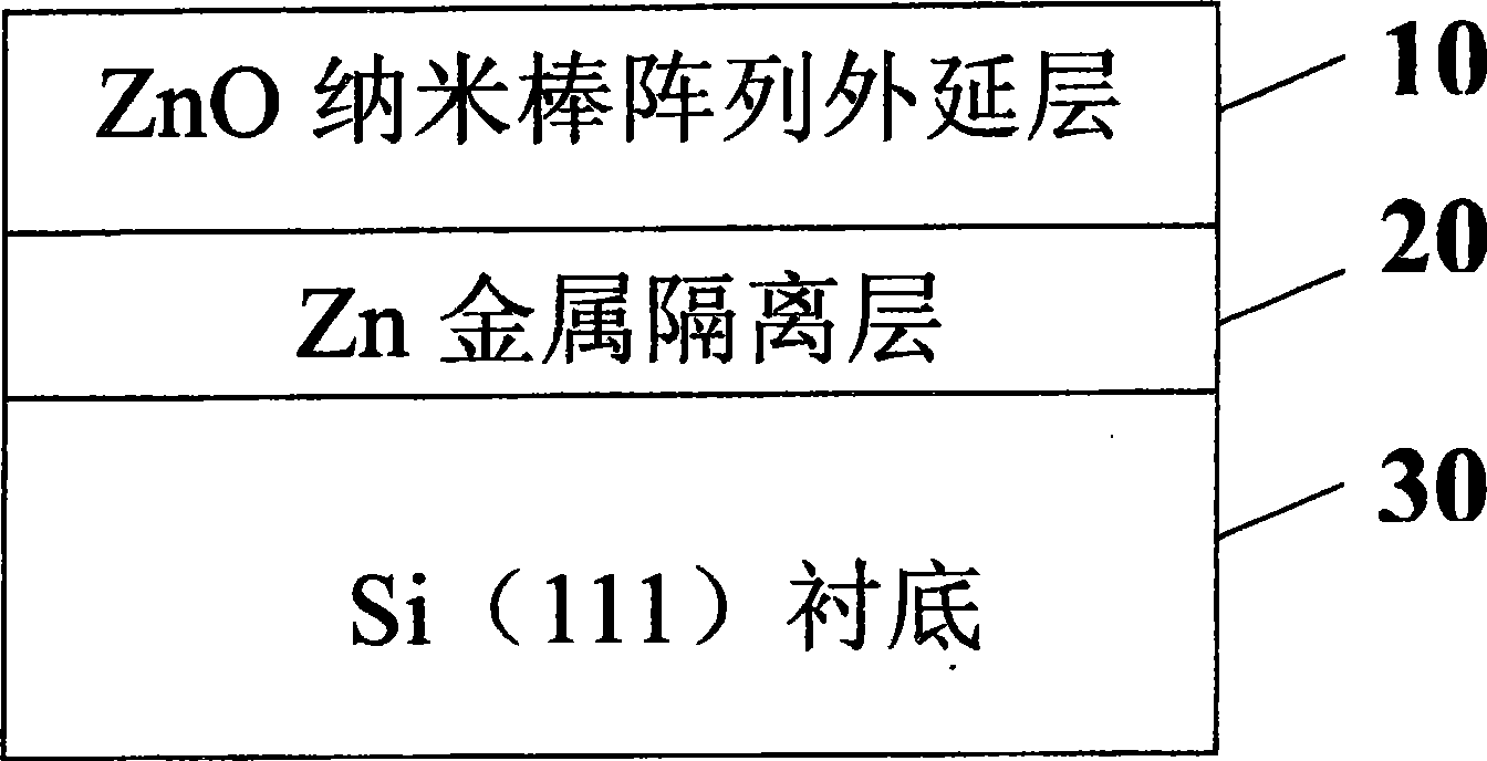
[0031] see again figure 1 Shown, key of the present invention is to solve the problem of growing high-quality ZnO nanorod array on Si substrate, it is characterized in that, comprises the steps:
[0032] Get a substrate 30, the substrate 30 is a Si substrate with large mismatch;
[0033] A thin Zn metal isolation layer 20 is grown on the Si(111) crystal plane on the substrate 30 by MOCVD method, the growth temperature is 600° C., and the reaction chamber pressure is 76 Torr. The pressure of the zinc organic source bottle is controlled at 800Torr, and the flow rate is controlled at 48SCCM;
[0034] Turn on the oxygen, control the flow rate at 1 SLM, and grow the ZnO nanorod array epitaxial layer 10 . Adjust the flow rate of oxygen carrier gas, control it at 8SLM, and the growth time is 30 minutes;
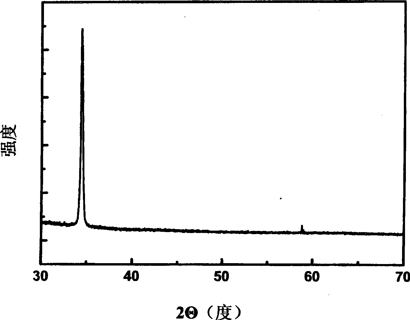
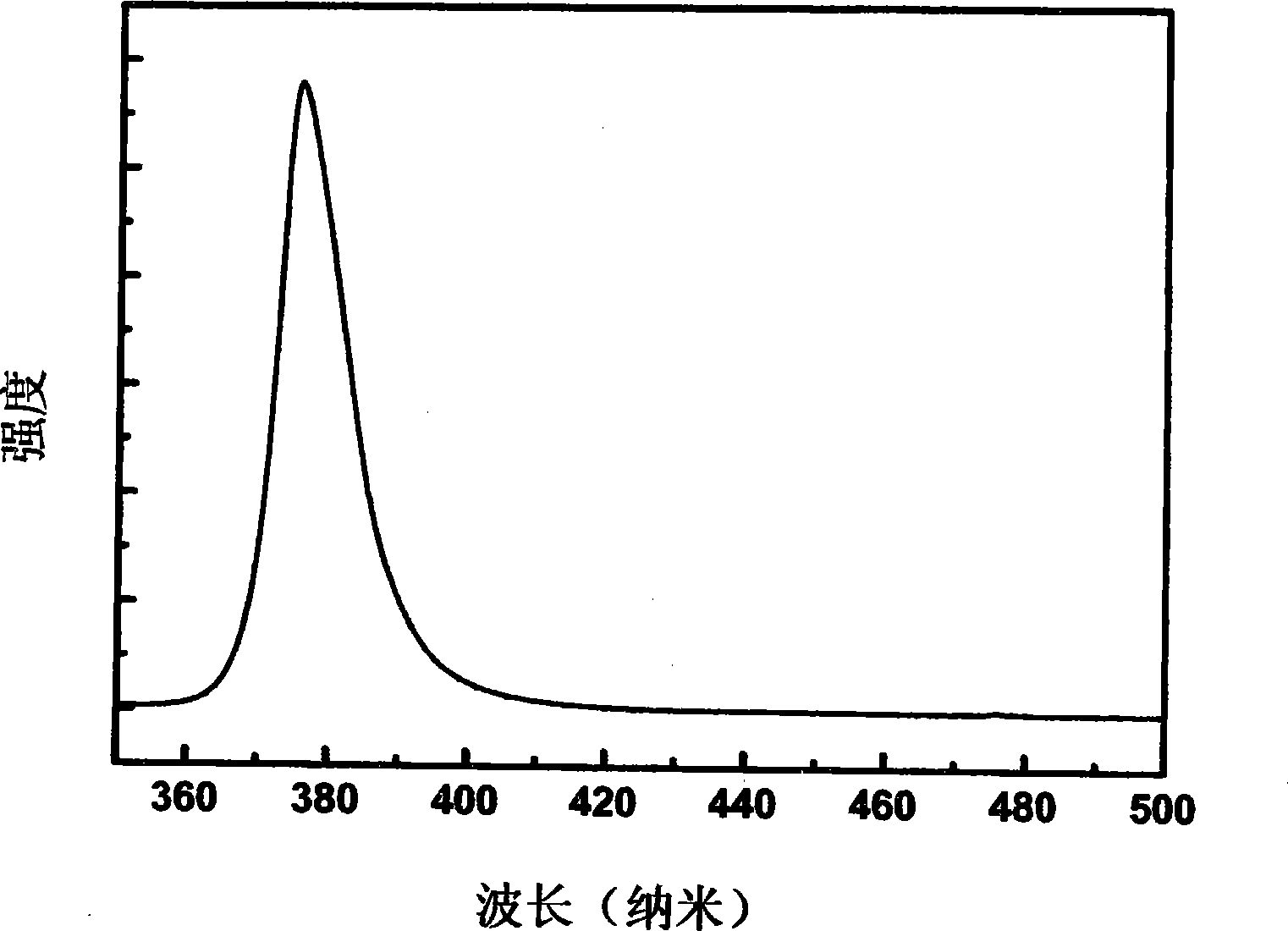
[0035] SEM, XRD and PL tests were performed on the ZnO nanorod arrays grown by the above method. The SEM photos show that the ZnO nanorod arrays are uniform in thickness, neatly...
PUM
 Abstract
Description
Claims
Application Information
 - R&D Engineer
- R&D Manager
- IP Professional
- Industry Leading Data Capabilities
- Powerful AI technology
- Patent DNA Extraction
Browse by: Latest US Patents, China's latest patents, Technical Efficacy Thesaurus, Application Domain, Technology Topic, Popular Technical Reports.
© 2024 PatSnap. All rights reserved.Legal|Privacy policy|Modern Slavery Act Transparency Statement|Sitemap|About US| Contact US: help@patsnap.com