NOR gate logic circuit and its forming method

A technology of logic circuits and NOT gates, applied in logic circuits, logic circuits with logic functions, circuits, etc., can solve problems that restrict the application of logic circuits

Active Publication Date: 2009-05-13
SOI MICRO CO LTD
View PDF0 Cites 5 Cited by
  • Summary
  • Abstract
  • Description
  • Claims
  • Application Information

AI Technical Summary

Problems solved by technology

However, since intrinsic ZnO is an N-type semiconductor, and most of the fabricated ZnO NW FETs are depletion-type devices, the application of ZnO nanowire materials to realize logic circuits based on enhancement / depletion-type FETs is restricted.

Method used


Image

  • NOR gate logic circuit and its forming method
  • NOR gate logic circuit and its forming method
  • NOR gate logic circuit and its forming method

Examples


Embodiment Construction

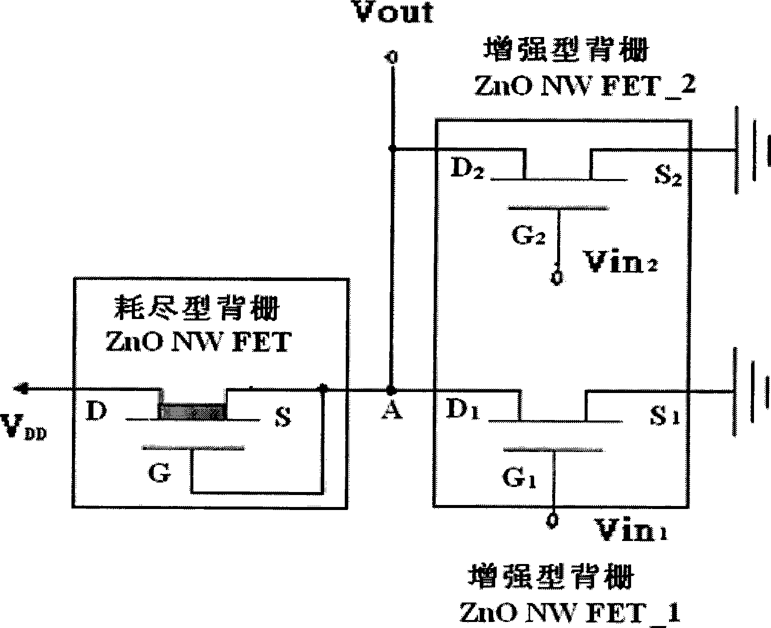
[0019] figure 1 It is a structural schematic diagram of a NOR gate logic circuit of the present invention. The NOR gate logic circuit, the first input terminal is used to receive the first input voltage signal Vin 1 ; The second input terminal is used to receive the second input voltage signal Vin 2 ; The first enhanced back gate zinc oxide nanowire field effect transistor (hereinafter expressed as: enhanced back gate ZnO NW FET_1), its gate electrode G 1 Coupled to the first input terminal, its source electrode S 1 Coupled to the ground point; the second enhanced back gate zinc oxide nanowire field effect transistor ZnO NWFET_2 (hereinafter expressed as: enhanced back gate ZnO NW FET_2), its gate electrode G 2 Coupled to the second input terminal, its source electrode S 2 Coupled to the ground point; a depletion-type back gate zinc oxide nanowire field effect transistor ZnO NW FET, and its drain electrode D is coupled to the voltage source ( figure 1 The medium voltage s...


PUM


Abstract

The invention relates to a NOR logic circuit and a fabricating method thereof. The NOR logic circuit comprises two input terminals, two enhancement type back-gate ZnO nanowire field effect transistors, and a depletion mode back-gate ZnO nanowire field effect transistor. The input terminals are respectively used for receiving input voltage signals; the gate electrodes of the two enhancement type back-gate ZnO nanowire field effect transistors are coupled to the two input terminals respectively, and the source electrodes thereof are coupled to an earth point respectively; the drain electrode of the depletion mode back-gate ZnO nanowire field effect transistor is coupled to a voltage source, and the gate electrode and the source electrode of the depletion mode back-gate ZnO nanowire field effect transistor, and the drain electrodes of the two enhancement type back-gate ZnO nanowire field effect transistors are coupled at a point; and the point serves as an output terminal used for outputting the voltage signals. The invention utilizes the manufacturing technology and the interconnection technology of ZnO nanowire materials and ZnO nanowire field effect transistors, and fabricates the NOR logic circuit based on the direct coupling field effect of the ZnO nanowire field effect transistor.

Description

technical field [0001] The invention relates to the field of compound semiconductor materials and devices, in particular to a NOR gate logic circuit based on a back-gate zinc oxide nanowire field-effect transistor (Direct-coupled FET Logic, referred to as DCFL) and its formation method. Background technique [0002] ZnO is a new type of multifunctional compound semiconductor material with direct bandgap of II-VI groups, and is called the third generation wide bandgap semiconductor material. The ZnO crystal has a wurtzite structure, the band gap is about 3.37eV, and the exciton binding energy is about 60meV. ZnO has the characteristics of semiconductor, photoelectricity, piezoelectricity, pyroelectricity, gas sensitivity and transparent conductivity, and has broad potential application value in many fields such as sensing, sound, light and electricity. [0003] In recent years, research on ZnO materials and devices has received extensive attention. The scope of research co...

Claims


Application Information

Patent Timeline
Patent Type & Authority Applications(China)
IPC IPC(8): H03K19/20H03K19/094H01L27/02H01L27/088H01L29/78H01L21/336
Inventor 徐静波张海英
Owner SOI MICRO CO LTD
Why Eureka
Try Eureka