Method for manufacturing semiconductor substrate, solar semiconductor substrate, and etching liquid

A manufacturing method and semiconductor technology, applied in the field of etching solution, can solve the problems of environmental safety, uneven shape and size of waste liquid treatment, etc., and achieve the effects of excellent photoelectric conversion efficiency, excellent stability and stable shape

Inactive Publication Date: 2009-05-13
MIMASU SEMICON IND CO LTD
View PDF3 Cites 4 Cited by
  • Summary
  • Abstract
  • Description
  • Claims
  • Application Information

AI Technical Summary

Problems solved by technology

However, because this method uses isopropyl alcohol, there are problems in waste liquid treatment, working environment, and safety. In addition, the shape and size of the unevenness are uneven, and it is difficult to form uniform fine unevenness in the surface.

Method used


Image

  • Method for manufacturing semiconductor substrate, solar semiconductor substrate, and etching liquid
  • Method for manufacturing semiconductor substrate, solar semiconductor substrate, and etching liquid
  • Method for manufacturing semiconductor substrate, solar semiconductor substrate, and etching liquid

Examples


experiment example 1

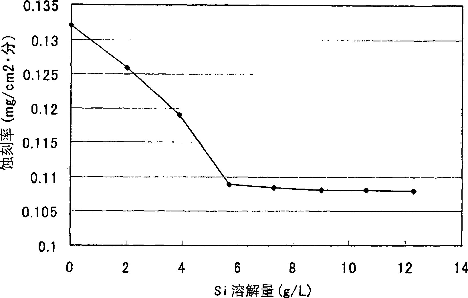
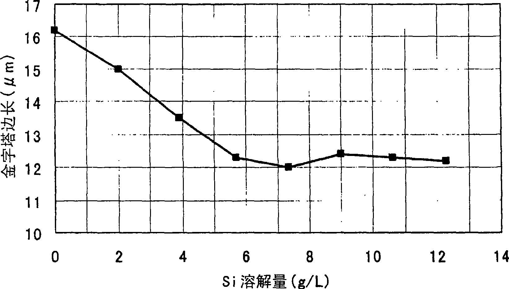
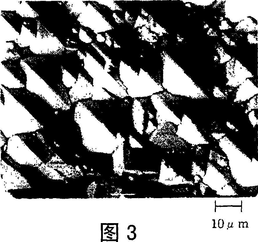
[0059] The etching solution is used to add 50g / L (0.43mol / L) hexanoic acid and a prescribed amount of potassium silicate (dissolved silicon: 0, 2.0, 3.9, 5.7, 7.3, 9.0, 10.6 Or 12.3g / L) etching solution, after immersing a single crystal silicon substrate (a square with a side of 126mm and a thickness of 200μm) with a (100) plane on the surface at 90°C for 30 minutes, the silicon substrate after the etching treatment was detected The dissolution loss, calculate the etch rate. In addition, the surface of the etched substrate was observed with a scanning electron microscope to detect the side length of the pyramid. In addition, here, the pyramid side length is the concavo-convex structure with a unit area of ​​265 μm × 200 μm, select 10 places from the larger one in order, detect the side lengths of the bottom surfaces of these pyramid structures, and take the average value of the side lengths ( the maximum side length of the base).

[0060] figure 1 It is a graph of the relat...

experiment example 2

[0063] Except that the concentration of the KOH aqueous solution was changed to 12.5% ​​by weight, the same experiment as in Experimental Example 1 was carried out to calculate the etching rate, and the same result as in Experimental Example 1 was obtained.

[0064] In addition, when the silicon dissolution amount was 5.7 g / L, the surface of the substrate after the etching treatment was observed with a scanning electron microscope, and the side length of the pyramid was detected, and the side length of the pyramid was 10 μm. The scanning electron microscope photo (magnification: 500 times) as Figure 7 shown.

experiment example 3

[0066] Except having used the etchant which added 50 g / L (0.35 mol / L) of octanoic acid instead of hexanoic acid, the same experiment as Experimental example 1 was implemented, and the etch rate was calculated. The result is as Figure 8 shown. like Figure 8 It was shown that the etching rate was stabilized by dissolving silicon in an alkaline solution to which octanoic acid was added.

[0067] In addition, when the silicon dissolution amount was 5.7 g / L, the etched substrate surface was observed with a scanning electron microscope, and the pyramid side length was detected, and the pyramid side length was 15 μm. Its scanning electron microscope photo (magnification: 500 times) such as Figure 9 shown.


PUM


Abstract

This invention provides a safe and low-cost semiconductor substrate manufacturing method, which can form a fine concave-convex structure, which can realize excellent photoelectric conversion, can realize stable etching rate and pyramid shape, and is suitable for solar batteries, in a desired size evenly on the surface of a semiconductor substrate. There are also provided a solar semiconductor substrate having an even and fine pyramid-shaped concave-convex structure evenly in a plane, and an etching liquid, which is highly stable in use in an early stage and can form a semiconductor substrate having an even and fine concave-convex structure. A semiconductor substrate is etched with an alkaline etching liquid containing at least one member, selected from the group consisting of carboxylic acids having 1 to 12 carbon atoms and containing at least one carboxyl group per molecule and their salts, and silicon to form a concave-convex structure on the surface of the semiconductor substrate.

Description

technical field [0001] The present invention relates to a method for manufacturing a semiconductor substrate having a concavo-convex structure used in solar cells and the like, a semiconductor substrate for solar energy, and an etchant used in the method. Background technique [0002] In recent years, in order to improve the efficiency of solar cells, a method of forming a concave-convex structure on the surface of the substrate and allowing incident light from the surface to enter the interior of the substrate with good efficiency has been adopted. The method of uniformly forming a fine concave-convex structure on the surface of the substrate, such as the method of Non-Patent Document 1, is to implement anisotropy using a mixed aqueous solution of sodium hydroxide and isopropanol on the surface of a single crystal silicon substrate having a (100) plane on the surface. Etching is a method of forming pyramid-shaped (square pyramid-shaped) concavities and convexities composed ...

Claims


Application Information

Patent Timeline
Patent Type & Authority Applications(China)
IPC IPC(8): H01L21/308H01L31/04
CPCH01L31/0236H01L31/18Y02E10/50H01L31/02363H01L31/04
Inventor 土屋正人真下郁夫木村义道
Owner MIMASU SEMICON IND CO LTD
Why Eureka
Try Eureka