Flat non down-lead encapsulation piece and method for producing the same

A flat leadless, production method technology, applied in electrical components, electrical solid-state devices, semiconductor devices, etc., can solve problems such as product delamination defects, performance degradation, and customer use troubles, and achieve significant anti-delamination defects and structural Simple and reasonable, the effect of improving packaging yield

Active Publication Date: 2009-05-27
TIANSHUI HUATIAN TECH
View PDF0 Cites 30 Cited by
  • Summary
  • Abstract
  • Description
  • Claims
  • Application Information

AI Technical Summary

Problems solved by technology

[0005] 1. The bonding force between the integrated circuit chip and the carrier is not good. When affected by changes in the external environment, it will cause layered defects inside the product, resulting in performance degradation or even failure;
[0006] 2. The bonding force between the back of the carrier and the plastic encapsulant is not good. When affected by the external environment, it will cause defects (delamination) in the product; or there is thicker flash on the exposed carrier (base island), which will cause subsequent flash removal. Create difficulties and increase the chance of delamination defects;
[0007] 3. The position of the first pin of the QFN appearance is not easy to distinguish, which brings unnecessary troubles to the packaging manufacturing process and customer use

Method used


Image

  • Flat non down-lead encapsulation piece and method for producing the same
  • Flat non down-lead encapsulation piece and method for producing the same
  • Flat non down-lead encapsulation piece and method for producing the same

Examples


Embodiment 1

[0070] 1. Wafer thinning / scribing

[0071] The thinning of the wafer packaged with a thickness of 0.75mm is the same as that of ordinary QFN plastic-encapsulated integrated circuits. First paste the adhesive film on the front of the wafer, and then thin it on a special thinning machine. The thickness of the wafer thinned is controlled at 180 μm.

[0072] 2. Core loading

[0073] The upper core adopts the following special frame:

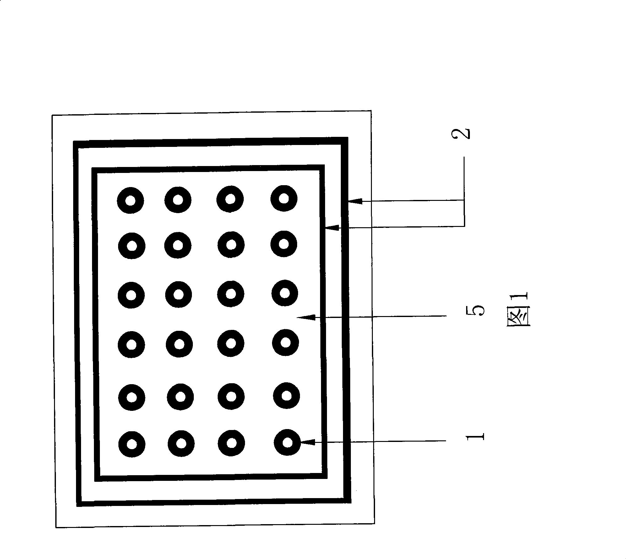
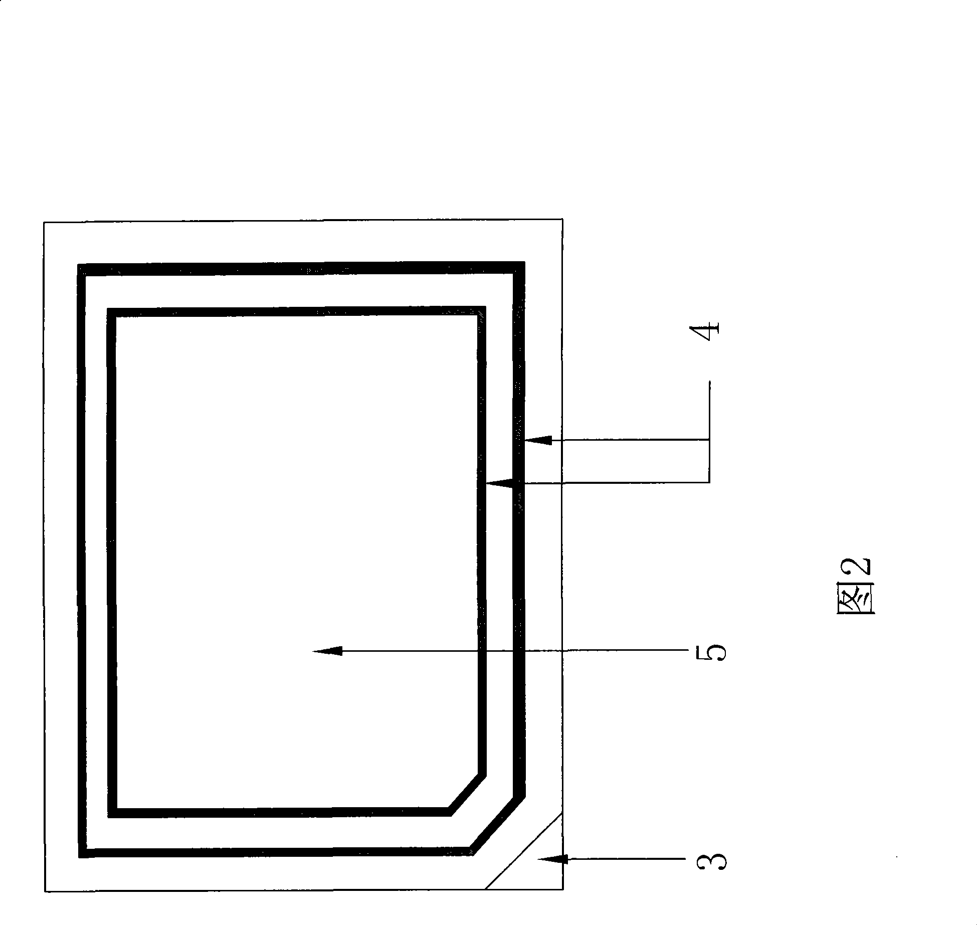
[0074] There are multiple rows of circular or trapezoidal pits 1 on the front of the lead frame carrier 5, and there are two circles of waterproof grooves 2 on the edge of the lead frame carrier; there is a 45-degree bevel at the lower right corner of the back of the carrier, as a PIN1 mark, and there are two circles on the edge of the carrier. Ring anti-overflow groove 4. At the same time, the back of the lead frame is pasted with an ordinary adhesive film when it leaves the factory.

[0075] The conductive adhesive, that is, the insulating adhe...

Embodiment 2

[0088] 1. Wafer thinning / scribing

[0089] For wafers packaged with a thickness of 0.5mm, the chip thickness is controlled between 130μm and 150μm. Anti-fragmentation and anti-warping thinning process control technology is adopted. Coarse grinding is used within the range of incoming wafer thickness + adhesive film thickness - 50μm thickness. Grinding speed ≤ 30μm / min; use fine grinding within the range of final wafer thickness + adhesive film thickness + 30μm, and fine grinding speed ≤ 10μm / min. In scribing, the scribing feed speed is ≤10mm / s, and a double-knife scribing machine is used if necessary.

[0090] 2. Core loading

[0091] The upper core adopts the following special frame:

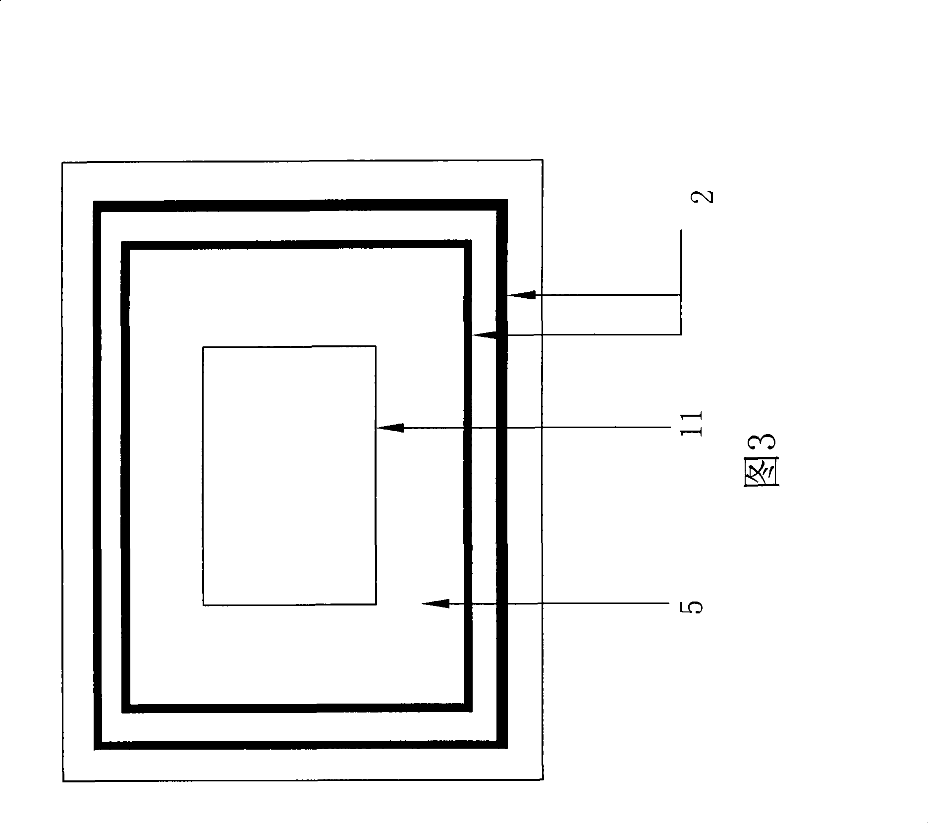
[0092] There is a rectangular or square pit 1 on the front of the lead frame carrier 5 , and the bottom surface of the pit 1 is flat. There are two circles of waterproof grooves 2 on the edge of the lead frame carrier. The lower right corner of the back of the lead frame carrier 5 is design...


PUM


Abstract

The invention discloses a flat non-lead packaging part and a production method thereof. The flat non-lead packaging part comprises a lead frame carrier, wherein the carrier is adhered with an IC chip. The front side of the lead frame carrier is provided with pits. The periphery of the front side of the lead frame carrier is provided with two circles of waterproof grooves. The back side of the lead frame carrier is provided two circles of anti-overflow grooves. The production method comprises the processes of washer thinning and slicing, core loading, press welding, plastic package, plating, printing and cutting and coiling. The method strengthens the bonding forces between the adhesive and the lead frame carrier and the IC chip and eliminates and reduces the rate of a lamination defect generated on the surface of the IC chip. The two circles of waterproof grooves are provided on the periphery of the carrier, the plastic packaging materials are embedded in the grooves so as to prevent moisture from entering the chip. The two circles of anti-overflow grooves arranged on the edge of the carrier have functions of preventing the lamination defect, moisture and material overflow. The method has the advantages of high rate of finished product, good reliability and convenient use, and effectively improves the reliability and excellent packaging rate of products.

Description

technical field [0001] The invention relates to the technical field of integrated circuit packaging, in particular to a flat leadless package capable of effectively preventing delamination defects, and also includes a plastic sealing production method of the flat leadless package. Background technique [0002] Delamination defects generated during the packaging process have become one of the main factors that reduce yield and affect reliability. Many customers not only require products to pass MSL 3, but also pass MSL 2 assessment, and even propose MSL1, no delamination. In addition, because the position of the first pin of the QFN appearance is not easy to distinguish, it brings unnecessary troubles to the packaging manufacturing process and customer use. [0003] Ordinary QFN packaging mainly has the following shortcomings: [0004] Because ordinary QFN packaging is only used for general products and does not have high reliability requirements, the lead frame used has no ...

Claims


Application Information

Patent Timeline
Patent Type & Authority Applications(China)
IPC IPC(8): H01L23/488H01L23/495H01L21/50
CPCH01L2224/32257H01L2224/48091H01L2224/73265H01L2224/32245H01L2224/48247H01L2224/45147H01L2224/83385H01L2924/181H01L2224/45124H01L2224/45144H01L2924/00014H01L2924/01014H01L2924/00012
Inventor 郭小伟慕蔚李习周
Owner TIANSHUI HUATIAN TECH
Why Eureka
Try Eureka